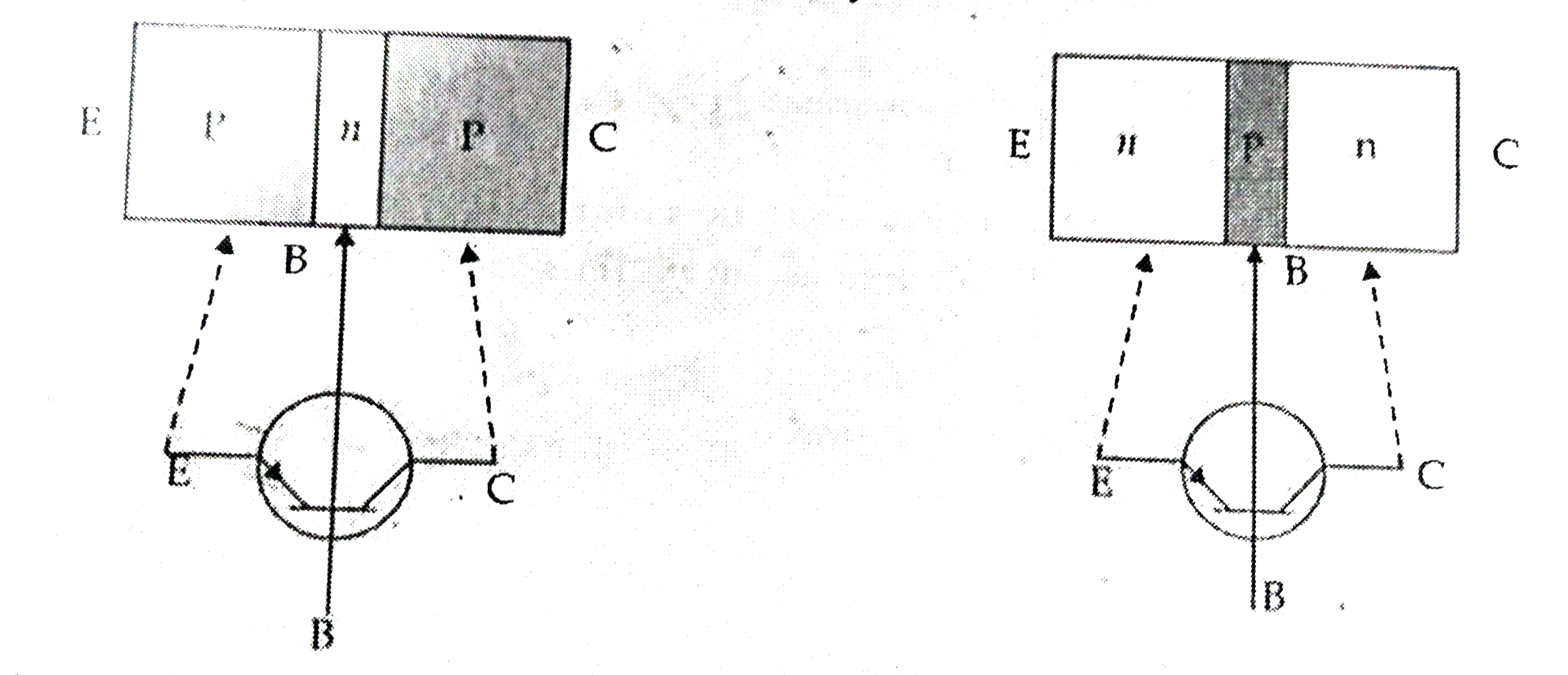
(a) Differentiate between three segments of a transistor on the basis of their size and level of doping.
(b) How is a transistor biased to be in active state?
(c) With the help of a necessary circuit diagram, describe briefly how n-p-n transistor in CE configuration amplifies a small sinusoidal input voltage. Write the expression for the ac current gain.
(a) Emitter (E) : It is the left hand side thick layer of the transistor, which is heavily doped.

Base (B) : It is the central thin layer of the transistor, which is lightly doped.
Collector (C) - It is the right hand side thick layer of the transistor, which is moderately dope.
(b) There are two conditions for a transistor to be into an active region.
1. The input circuit should be forwed biased by using a low voltage battery.
2. The output circuit should be reverse biased by using a high voltage battery.
(c) C.E. configuration (Transistor as an Amplifier). The current diagram of a common emitter amplifier using n-p-n transistor is shown in Figure.

The input (base-emitter) circuit is forwed biased and the output (collector-emiiter) circuit is reverse blased.
When no a.c. signal is applied, the potential difference between the collector and emitter is given by
.
When an a.c. signal is fed to the input circuit, the forward bias increases during the positive half cycle of the input. This results in increases in and decrease in . Thus, during positive half cycle of the input, the collector becomes less positive.
During the negative half cycle of the input, the forward bias is decreased resulting in decrease in and hence . Thus would increase making the collector more positive. Hence in a common-emitter amplifier, the output voltage is out of phase with the input voltage.
(i) Input signal voltage .
(ii) Output signal voltage .
(iii) Voltage gain of the amplifier is
Topper's Solved these Questions
- XII BOARDSBook:XII BOARD PREVIOUS YEAR PAPER ENGLISHChapter:XII BOARDSExercise:[SET - II DELHI BOARD]
Explore 5 Videos
- XII BOARDSBook:XII BOARD PREVIOUS YEAR PAPER ENGLISHChapter:XII BOARDSExercise:[SET - III, DELHI BOARD]
Explore 6 Videos
- XII BOARDSBook:XII BOARD PREVIOUS YEAR PAPER ENGLISHChapter:XII BOARDSExercise:SET-II
Explore 33 Videos
- SAMPLE PAPER 2019Book:XII BOARD PREVIOUS YEAR PAPER ENGLISHChapter:SAMPLE PAPER 2019Exercise:SECTION D
Explore 6 Videos
Similar Questions
Give a circuit diagram of a common emitter amplifier using an n-p-n transistor. Draw the input and output wavefroms of the signal. Write the expression for its voltage gain.
View SolutionDraw a circuit diagram of n−p transistor amplifier in CE configuration. Under what condition does the transistor acts as an amplifier?
View SolutionDraw a circuit diagram of C.E. transistor amplifier. Briefly explain its working and write the expression for (i) current gain (ii) voltage gain of the amplifier.
View SolutionDraw a labelled circuit diagram of n - p - n germanium transistor in common emitter configuration. Explain briefly, how this transistor is used as a voltage amplifier.
View Solution(i) Draw a circuit diagram to study the input and output characteristics of an n-p-n transistor in its common emitter configuration. Draw the typical input and output characteristics.
(ii) Explain, with the hepl of a circuit diagram, the working of n-p-n transistor as a common emitter amplifier.
View SolutionDescribe briefly the functions of the three segments of n-p-n transistor.
View SolutionDescribe briefly with the help of a circuit diagram, how the flow of current carriers in a p-n-p transistor is regulated with emitter-base junction forward biased and base-collector junction reverse biased.
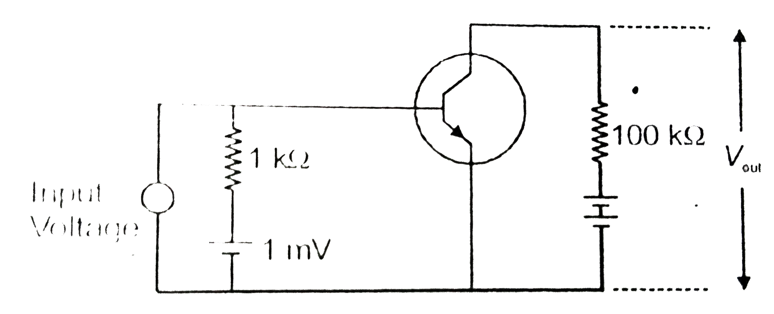
View SolutionIn the following common emitter configuration an n-p-n transistor with current gain β=100 is used. What is the output voltage of the amplifier ?

View Solution(i) Write the functions of three segments of a transistor.
(ii) Draw the ciruit diagram or studying the input and output characteristics of n-p-n transisfor in common emitter configuration . Using the circuit explain how input characteristics are obtained .
View SolutionDraw the typical input and output characterisitics of an n-p-n transistor in CE configurtion . Show how these characteristic can be used to determine (a) the input resistance (r1) and (b) current amplification factor (β).
View Solution

