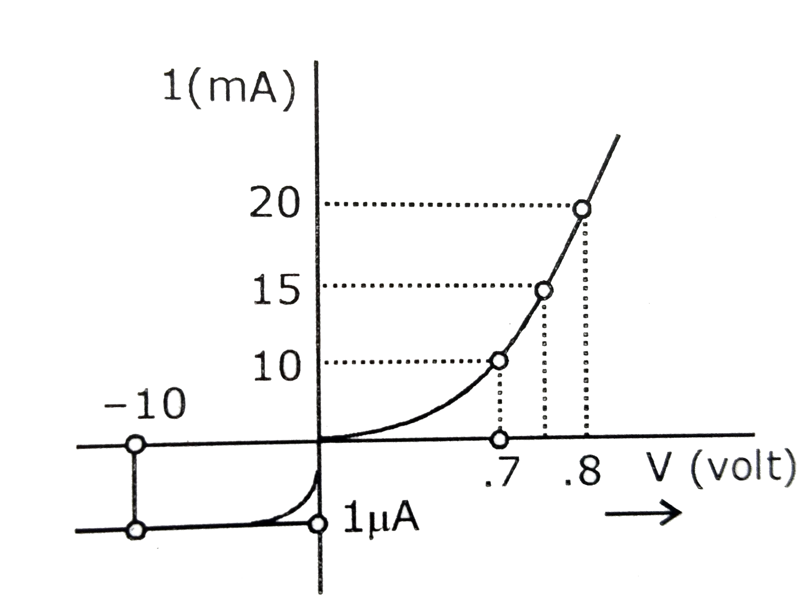
Using the necessary circuit diagram, show how the V-I characteristics of a p-n junction are obtained in (i) forward biasing (ii) Reverse biasing. How are these characteristics made use of in rectification?
To solve the question regarding the V-I characteristics of a p-n junction in forward and reverse biasing, and how these characteristics are utilized in rectification, we will follow a structured approach.
Step 1: Understanding the p-n Junction
A p-n junction is formed by joining p-type and n-type semiconductors. The p-side has an abundance of holes (positive charge carriers), while the n-side has an abundance of electrons (negative charge carriers).
Step 2: Circuit Diagram for Forward Biasing
1. Circuit Setup:
- Connect the positive terminal of a voltage source to the p-side of the diode and the negative terminal to the n-side.
- This configuration allows current to flow through the diode.
Diagram:
+V−−−−−−∣>⊢−−−−−Diode
Step 3: V-I Characteristics in Forward Biasing
1. Current Flow: When forward biased, the applied voltage reduces the potential barrier, allowing current to flow. The current increases exponentially with the increase in voltage.
2. Graph: Plot the voltage (V) on the x-axis and the current (I) on the y-axis. The graph will show a sharp increase in current after a certain threshold voltage (typically around 0.7V for silicon diodes).
Graph:
I∣∣|/||/|/∣∣∣∠__________V
Step 4: Circuit Diagram for Reverse Biasing
1. Circuit Setup:
- Connect the positive terminal of the voltage source to the n-side of the diode and the negative terminal to the p-side.
- This configuration prevents current from flowing through the diode.
Diagram:
−V−−−−−−∣<⊢−−−−+Diode
Step 5: V-I Characteristics in Reverse Biasing
1. Current Flow: In reverse bias, the potential barrier is increased, and only a very small reverse saturation current flows until the breakdown voltage is reached.
2. Graph: The graph will show a small current (reverse saturation current) until the breakdown voltage, after which the current increases sharply.
Graph:
I|||∣|||||/||/⌊__⌋__________V
Step 6: Rectification Using V-I Characteristics
1. Forward Bias: In forward bias, the diode conducts current, allowing AC to be converted to DC.
2. Reverse Bias: In reverse bias, the diode blocks current, preventing negative cycles of AC from passing through.
3. Application: This property is utilized in rectifiers, which convert alternating current (AC) to direct current (DC).
A p-n junction is formed by joining p-type and n-type semiconductors. The p-side has an abundance of holes (positive charge carriers), while the n-side has an abundance of electrons (negative charge carriers).
1. Circuit Setup:
- Connect the positive terminal of a voltage source to the p-side of the diode and the negative terminal to the n-side.
- This configuration allows current to flow through the diode.
+V−−−−−−∣>⊢−−−−−Diode
1. Current Flow: When forward biased, the applied voltage reduces the potential barrier, allowing current to flow. The current increases exponentially with the increase in voltage.
2. Graph: Plot the voltage (V) on the x-axis and the current (I) on the y-axis. The graph will show a sharp increase in current after a certain threshold voltage (typically around 0.7V for silicon diodes).
I∣∣|/||/|/∣∣∣∠__________V
1. Circuit Setup:
- Connect the positive terminal of the voltage source to the n-side of the diode and the negative terminal to the p-side.
- This configuration prevents current from flowing through the diode.
−V−−−−−−∣<⊢−−−−+Diode
1. Current Flow: In reverse bias, the potential barrier is increased, and only a very small reverse saturation current flows until the breakdown voltage is reached.
2. Graph: The graph will show a small current (reverse saturation current) until the breakdown voltage, after which the current increases sharply.
I|||∣|||||/||/⌊__⌋__________V
1. Forward Bias: In forward bias, the diode conducts current, allowing AC to be converted to DC.
2. Reverse Bias: In reverse bias, the diode blocks current, preventing negative cycles of AC from passing through.
3. Application: This property is utilized in rectifiers, which convert alternating current (AC) to direct current (DC).
Topper's Solved these Questions
- XII BOARDSBook:XII BOARD PREVIOUS YEAR PAPER ENGLISHChapter:XII BOARDSExercise:[SET - II DELHI BOARD]
Explore 5 Videos
- XII BOARDSBook:XII BOARD PREVIOUS YEAR PAPER ENGLISHChapter:XII BOARDSExercise:[SET - III, DELHI BOARD]
Explore 6 Videos
- XII BOARDSBook:XII BOARD PREVIOUS YEAR PAPER ENGLISHChapter:XII BOARDSExercise:SET-II
Explore 33 Videos
- SAMPLE PAPER 2019Book:XII BOARD PREVIOUS YEAR PAPER ENGLISHChapter:SAMPLE PAPER 2019Exercise:SECTION D
Explore 6 Videos
Similar Questions
What happens to the width of depletion layer of a p-n junction when it is (i) forward biased, (ii) reverse biased?
View SolutionThe resistance of p-n junction is low when forward biased and is high when reverse biased. Explain.
View SolutionForward bias characteristics of a p -n junction diode is used in which of the following devices ?
View SolutionDraw the circuit diagram of a half - wave rectifier using a p-n junction diode.
View SolutionThe V-I characteristic of a diode is shown in the figure. The ratio of forward to reverse bias resistance is

View SolutionThe V-I characteristic of a diode is shown in the figure. The ratio of forward to reverse bias resistance is

View SolutionHow is forward biasing different from reverse biasing in a p-n junction diode?
View SolutionDraw typical output characteristics of an n-p-n transistor in CE configuration. Show how these characteristics can be used to determine output resistance.
View SolutionIn V-I characteristics of a p-n junction diode, why is the current under reverse bias almost independent of the applied potential upto a critical voltage?
View Solution(i) Write the functions of three segments of a transistor.
(ii) Draw the ciruit diagram or studying the input and output characteristics of n-p-n transisfor in common emitter configuration . Using the circuit explain how input characteristics are obtained .
View Solution

