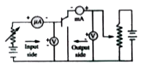
Draw a labelled circuit diagram of n - p - n germanium transistor in common emitter configuration. Explain briefly, how this transistor is used as a voltage amplifier.
Step-by-Step Solution:
Step 1: Draw the Circuit Diagram
1. Begin by drawing the NPN transistor in the center of your diagram.
2. Label the three terminals of the transistor: Collector (C), Base (B), and Emitter (E).
3. Connect the Collector to a positive voltage supply (VCC).
4. Connect the Emitter to the ground.
5. Connect a resistor (RC) between the Collector and VCC to limit the current.
6. Connect a resistor (RE) between the Emitter and ground to stabilize the transistor.
7. Connect the Base to the input signal (VI) through a coupling capacitor (C1) to block DC.
8. Connect a biasing voltage (VBB) to the Base through another resistor (RB) to ensure proper biasing.
Step 2: Explain the Functioning of the NPN Transistor as a Voltage Amplifier
1. Biasing: The voltage VBB is applied to the Base terminal to ensure that the transistor is in the active region. This is crucial for amplification.
2. Input Signal: The input signal (VI) is applied between the Base and Emitter. This small input signal modulates the Base current (IB).
3. Current Amplification: A small change in the Base current (IB) leads to a larger change in the Collector current (IC) due to the transistor's current gain (β). The relationship can be expressed as:
IC=β⋅IB
4. Output Voltage: The output voltage (VO) is taken across the load connected to the Collector. As the Collector current increases, the voltage drop across the load resistor (RC) increases, leading to a larger output voltage.
5. Phase Shift: The output signal is inverted (180 degrees out of phase) compared to the input signal due to the nature of the transistor operation.
Final Circuit Diagram
- The final circuit diagram should clearly show the NPN transistor with all connections labeled, including VCC, VBB, VI, RC, RE, and RB.
Summary
In summary, the NPN germanium transistor in common emitter configuration acts as a voltage amplifier by using a small input current to control a larger output current, resulting in a larger output voltage that is inverted relative to the input.
---
1. Begin by drawing the NPN transistor in the center of your diagram.
2. Label the three terminals of the transistor: Collector (C), Base (B), and Emitter (E).
3. Connect the Collector to a positive voltage supply (VCC).
4. Connect the Emitter to the ground.
5. Connect a resistor (RC) between the Collector and VCC to limit the current.
6. Connect a resistor (RE) between the Emitter and ground to stabilize the transistor.
7. Connect the Base to the input signal (VI) through a coupling capacitor (C1) to block DC.
8. Connect a biasing voltage (VBB) to the Base through another resistor (RB) to ensure proper biasing.
1. Biasing: The voltage VBB is applied to the Base terminal to ensure that the transistor is in the active region. This is crucial for amplification.
2. Input Signal: The input signal (VI) is applied between the Base and Emitter. This small input signal modulates the Base current (IB).
3. Current Amplification: A small change in the Base current (IB) leads to a larger change in the Collector current (IC) due to the transistor's current gain (β). The relationship can be expressed as:
IC=β⋅IB
4. Output Voltage: The output voltage (VO) is taken across the load connected to the Collector. As the Collector current increases, the voltage drop across the load resistor (RC) increases, leading to a larger output voltage.
5. Phase Shift: The output signal is inverted (180 degrees out of phase) compared to the input signal due to the nature of the transistor operation.
- The final circuit diagram should clearly show the NPN transistor with all connections labeled, including VCC, VBB, VI, RC, RE, and RB.
In summary, the NPN germanium transistor in common emitter configuration acts as a voltage amplifier by using a small input current to control a larger output current, resulting in a larger output voltage that is inverted relative to the input.
Topper's Solved these Questions
- XII BOARDSBOOK - XII BOARD PREVIOUS YEAR PAPER ENGLISHCHAPTER - XII BOARDSEXERCISE - SECTION - D
3 Videos
- XII BOARDSBOOK - XII BOARD PREVIOUS YEAR PAPER ENGLISHCHAPTER - XII BOARDSEXERCISE - SECTION - E
5 Videos
- XII BOARDSBOOK - XII BOARD PREVIOUS YEAR PAPER ENGLISHCHAPTER - XII BOARDSEXERCISE - [SET -III, OUTSIDE DELHI]
3 Videos
- SAMPLE PAPER 2019BOOK - XII BOARD PREVIOUS YEAR PAPER ENGLISHCHAPTER - SAMPLE PAPER 2019EXERCISE - SECTION D
6 Videos
Similar Questions
When N-P-N transistor is used as an amplifier-
View SolutionDraw a labelled circuit diagram of a transistor acting as a common emitter amplifier. What is meant by phase reversal?
View SolutionDraw a labelled circuit diagram of a transistor as a switch and draw its input and output graphs.
View SolutionDraw the labelled circuit diagram of a common-emitter transistor amplifier : Explain clearly how the input and output signals are in opposite phase.
View SolutionThe symbol of p-n-p transistor is
View SolutionDraw a circuit diagram of n−p transistor amplifier in CE configuration. Under what condition does the transistor acts as an amplifier?
View Solution(i) Write the functions of three segments of a transistor.
(ii) Draw the ciruit diagram or studying the input and output characteristics of n-p-n transisfor in common emitter configuration . Using the circuit explain how input characteristics are obtained .
View Solution(i) Draw a circuit diagram to study the input and output characteristics of an n-p-n transistor in its common emitter configuration. Draw the typical input and output characteristics.
(ii) Explain, with the hepl of a circuit diagram, the working of n-p-n transistor as a common emitter amplifier.
View SolutionIn the following common emitter configuration an n-p-n transistor with current gain β=100 is used. What is the output voltage of the amplifier ?

View SolutionThe circuit diagram below shows n-p-n transistor in CE configuration. For this configuration, mark the correct statement(s).

View Solution
