(a) Explain with the help of suitable diagram , the two processes which occur during the formations of a p -n junction diode . Hence , define the terms :
(i) depletion region and (ii) potential barrier :
(b) Draw a circuit diagram of a p - n junction diode under forward bias and explain its working .
Step-by-Step Solution
1. Understanding the p-n Junction:
- A p-n junction diode is formed by joining p-type and n-type semiconductors. The p-type semiconductor has an abundance of holes (positive charge carriers), while the n-type semiconductor has an abundance of electrons (negative charge carriers).
2. Diffusion Process:
- When the p-type and n-type materials are brought together, holes from the p-side will diffuse into the n-side, and electrons from the n-side will diffuse into the p-side. This movement occurs due to the concentration gradient, where charge carriers move from regions of high concentration to low concentration.
3. Recombination:
- As holes diffuse into the n-region, they recombine with electrons, and similarly, electrons from the n-region recombine with holes in the p-region. This leads to a reduction in the number of free charge carriers near the junction.
4. Formation of the Depletion Region:
- The recombination of charge carriers creates a region around the junction that is depleted of free charge carriers. This region is known as the depletion region. It contains fixed positive ions in the n-region and fixed negative ions in the p-region.
5. Creation of the Potential Barrier:
- The separation of charges in the depletion region creates an electric field, which establishes a potential difference across the junction. This potential difference is referred to as the potential barrier (V0). This barrier prevents further diffusion of charge carriers unless an external voltage is applied.
Diagram:
- Draw a diagram showing the p-n junction with labeled regions (p-region, n-region, depletion region) and indicate the movement of holes and electrons.
Definitions:
- Depletion Region: The area around the p-n junction where mobile charge carriers (holes and electrons) have recombined, leaving behind fixed positive and negative ions. This region is devoid of free charge carriers.
- Potential Barrier: The electric potential difference created across the depletion region due to the separation of charges. It opposes the further movement of charge carriers across the junction.
---
(b) Circuit Diagram of a p-n Junction Diode Under Forward Bias
1. Circuit Setup:
- Connect a battery to the p-n junction diode. The positive terminal of the battery is connected to the p-region, and the negative terminal is connected to the n-region.
2. Forward Bias Condition:
- In this configuration, the applied voltage from the battery is greater than the potential barrier (V0). This reduces the width of the depletion region and allows charge carriers to move across the junction.
3. Movement of Charge Carriers:
- Holes from the p-region are pushed towards the n-region, while electrons from the n-region are pushed towards the p-region. This movement leads to recombination of holes and electrons, allowing current to flow through the diode.
4. Induced Current:
- The flow of holes and electrons constitutes the induced current (ID) in the circuit. The direction of the current is taken as the direction of hole movement.
Diagram:
- Draw the circuit diagram showing the p-n junction diode with the battery connected in forward bias, indicating the direction of current flow.
---
- A p-n junction diode is formed by joining p-type and n-type semiconductors. The p-type semiconductor has an abundance of holes (positive charge carriers), while the n-type semiconductor has an abundance of electrons (negative charge carriers).
- When the p-type and n-type materials are brought together, holes from the p-side will diffuse into the n-side, and electrons from the n-side will diffuse into the p-side. This movement occurs due to the concentration gradient, where charge carriers move from regions of high concentration to low concentration.
- As holes diffuse into the n-region, they recombine with electrons, and similarly, electrons from the n-region recombine with holes in the p-region. This leads to a reduction in the number of free charge carriers near the junction.
- The recombination of charge carriers creates a region around the junction that is depleted of free charge carriers. This region is known as the depletion region. It contains fixed positive ions in the n-region and fixed negative ions in the p-region.
- The separation of charges in the depletion region creates an electric field, which establishes a potential difference across the junction. This potential difference is referred to as the potential barrier (V0). This barrier prevents further diffusion of charge carriers unless an external voltage is applied.
- Draw a diagram showing the p-n junction with labeled regions (p-region, n-region, depletion region) and indicate the movement of holes and electrons.
- Depletion Region: The area around the p-n junction where mobile charge carriers (holes and electrons) have recombined, leaving behind fixed positive and negative ions. This region is devoid of free charge carriers.
- Potential Barrier: The electric potential difference created across the depletion region due to the separation of charges. It opposes the further movement of charge carriers across the junction.
- Connect a battery to the p-n junction diode. The positive terminal of the battery is connected to the p-region, and the negative terminal is connected to the n-region.
- In this configuration, the applied voltage from the battery is greater than the potential barrier (V0). This reduces the width of the depletion region and allows charge carriers to move across the junction.
- Holes from the p-region are pushed towards the n-region, while electrons from the n-region are pushed towards the p-region. This movement leads to recombination of holes and electrons, allowing current to flow through the diode.
- The flow of holes and electrons constitutes the induced current (ID) in the circuit. The direction of the current is taken as the direction of hole movement.
- Draw the circuit diagram showing the p-n junction diode with the battery connected in forward bias, indicating the direction of current flow.
Topper's Solved these Questions
- XII BOARDSBOOK - XII BOARD PREVIOUS YEAR PAPER ENGLISHCHAPTER - XII BOARDSEXERCISE - SECTION - C
10 Videos
- XII BOARDSBOOK - XII BOARD PREVIOUS YEAR PAPER ENGLISHCHAPTER - XII BOARDSEXERCISE - SECTION - A
7 Videos
- XII BOARDSBOOK - XII BOARD PREVIOUS YEAR PAPER ENGLISHCHAPTER - XII BOARDSEXERCISE - SECTION - D
3 Videos
- SAMPLE PAPER 2019BOOK - XII BOARD PREVIOUS YEAR PAPER ENGLISHCHAPTER - SAMPLE PAPER 2019EXERCISE - SECTION D
6 Videos
Similar Questions
Knowledge Check
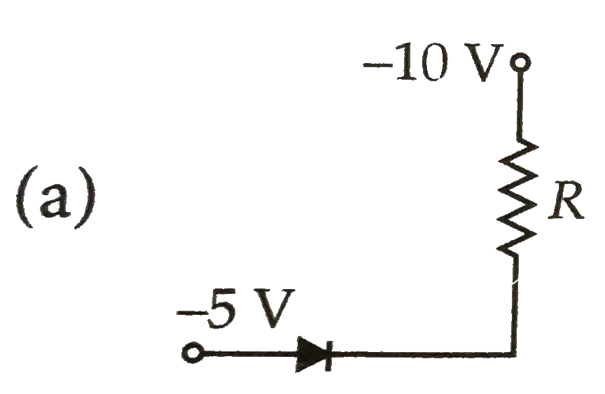
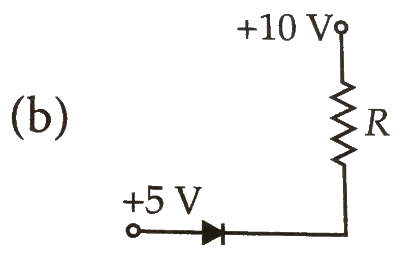
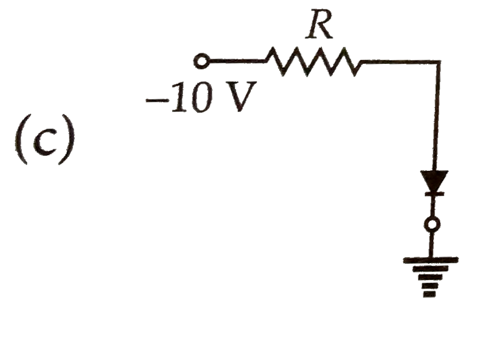
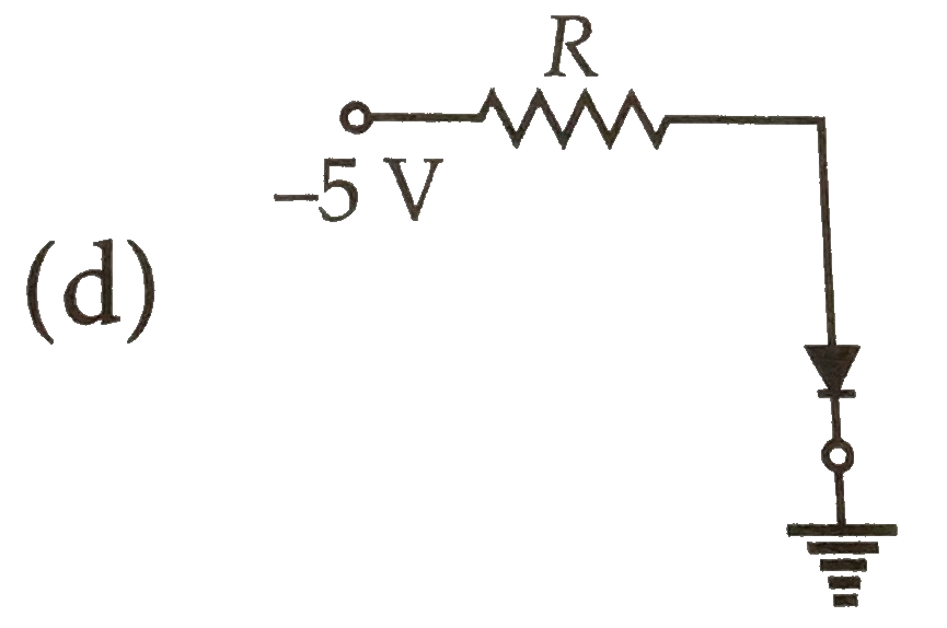
Which of the junction diodes shown below are forward biased ?
A B
B C
C D
D
When p−n junction diode is forward biased then
View SolutionWhen p−n junction diode is forward biased then
View Solutionp-n junction is called as forward biased when
View Solutionp−n junction diode can be used as
View SolutionA p−n junction diode is reverse biased. Then
View SolutionExplain the formation of depletion layer and potential barrier in p-n junction.
Draw the circuit diagram of a half wave rectifier and explain its working.
View SolutionIn forward biasing of the p-n junction:
View Solution
