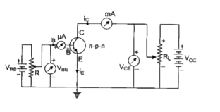
(i) Draw a circuit diagram to study the input and output characteristics of an n-p-n transistor in its common emitter configuration. Draw the typical input and output characteristics.
(ii) Explain, with the hepl of a circuit diagram, the working of n-p-n transistor as a common emitter amplifier.
Similar Questions
Explain with the help of a circuit diagram, the working of a p−n junction diode as a half wave rectifier.
View SolutionDraw typical output characteristics of an n-p-n transistor in CE configuration. Show how these characteristics can be used to determine output resistance.
View Solution(i) Write the functions of three segments of a transistor.
(ii) Draw the ciruit diagram or studying the input and output characteristics of n-p-n transisfor in common emitter configuration . Using the circuit explain how input characteristics are obtained .
View Solution(a) Draw the circuit arrangement for studying the input and output characteristics of an n-p-n transistor in CE configuration . With the help of these characteristics define (i) input resistance , (ii) current amplification factor .
(b) Describe briefly with the help of a circuit diagram how an n-p-n transistor is used to produce self-sustained oscillations .
View SolutionWhen N-P-N transistor is used as an amplifier-
View SolutionDraw the diagram of the circuit arangement used for studying the 'input' and the 'output' characteristics of an n-p-n transistor inits CE configuration. Briefly explain how these two types of characteristics are obtained and draw these characteristics.
(b) 'Define' the terms (i) Input resistance, (ii) Output resistance , (iii) Current amplification factor, for a given transistor.
View SolutionDraw a labelled circuit diagram of n - p - n germanium transistor in common emitter configuration. Explain briefly, how this transistor is used as a voltage amplifier.
View SolutionDraw the typical input and output characterisitics of an n-p-n transistor in CE configurtion . Show how these characteristic can be used to determine (a) the input resistance (r1) and (b) current amplification factor (β).
View SolutionDraw a labelled circuit diagram of a transistor acting as a common emitter amplifier. What is meant by phase reversal?
View SolutionIn a common emitter amplifier, the input and output voltage are out of phase by
View Solution

