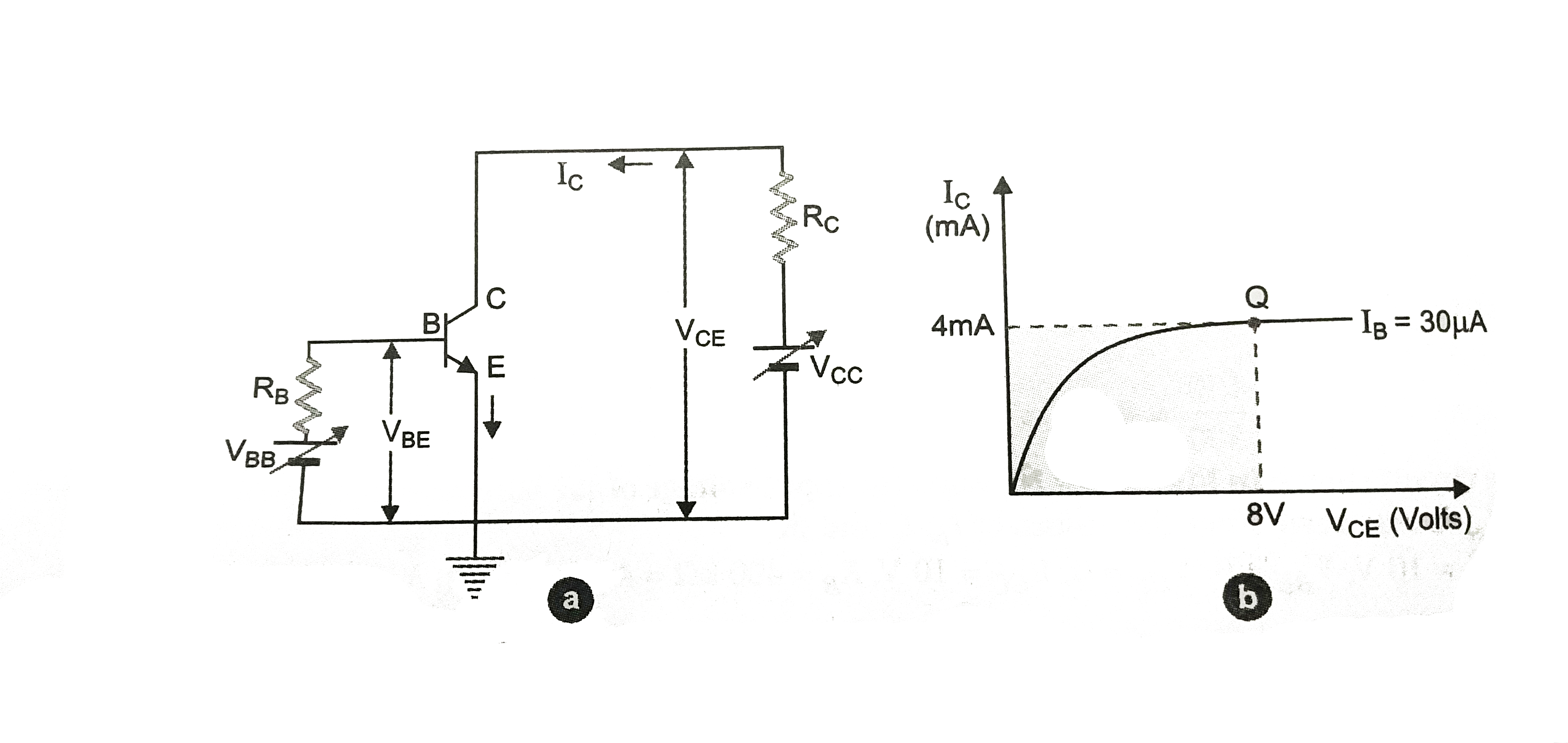
Draw the diagram of the circuit arangement used for studying the 'input' and the 'output' characteristics of an n-p-n transistor inits CE configuration. Briefly explain how these two types of characteristics are obtained and draw these characteristics.
(b) 'Define' the terms (i) Input resistance, (ii) Output resistance , (iii) Current amplification factor, for a given transistor.
(a) N/A
(i) The input resistance ri of the transistor in CE configuration is defined as the ratio of the small change in base -emitter voltage to the corresponding small change in the base current, when the collector-emitter voltage is kept fixed. Thus.
ri[ΔVBEΔIB]VCE=constant.
(ii) The output resistance r0 of a transistor in CE configuaration is definded as the ratio of the small change in the collector-emitter voltage to the corresponding change in the collector current when the base current is kept constant. Thus, r0[ΔVCEΔIC]IB=constant .
(ii) Current amplification factor (β) : It is defined as the ratio of the change in collector current to the small change in base current at constant collector-emitter voltage (VCE) when the transistor is in the acitve state.
βac=[ΔICΔIB]VCE=constant
Similar Questions
Draw typical output characteristics of an n-p-n transistor in CE configuration. Show how these characteristics can be used to determine output resistance.
View SolutionDescribe briefly the functions of the three segments of n-p-n transistor.
View Solution(a) Draw the circuit arrangement for studying the input and output characteristics of an n-p-n transistor in CE configuration . With the help of these characteristics define (i) input resistance , (ii) current amplification factor .
(b) Describe briefly with the help of a circuit diagram how an n-p-n transistor is used to produce self-sustained oscillations .
View Solution(i) Write the functions of three segments of a transistor.
(ii) Draw the ciruit diagram or studying the input and output characteristics of n-p-n transisfor in common emitter configuration . Using the circuit explain how input characteristics are obtained .
View SolutionDraw the typical input and output characterisitics of an n-p-n transistor in CE configurtion . Show how these characteristic can be used to determine (a) the input resistance (r1) and (b) current amplification factor (β).
View Solution(i) Draw a circuit diagram to study the input and output characteristics of an n-p-n transistor in its common emitter configuration. Draw the typical input and output characteristics.
(ii) Explain, with the hepl of a circuit diagram, the working of n-p-n transistor as a common emitter amplifier.
View SolutionConsider the circuit arrangnent shown in Fig. for studying input and output characteristics of npn transistor in CE configuration.
Select the values of R and R for a transistor whose VBE=0.7V, so that the transistor is operating at point Q as shown in the characteristics shown in Fig.
 Given that the input impedance of the transistor is very small and VCC=VBB=16V, also find the voltage gain and power gain of circuit making appropriate assumptions.
View SolutionInput characteristics are shown for CE configuration of n-p-n transistor for different output voltage. Here.

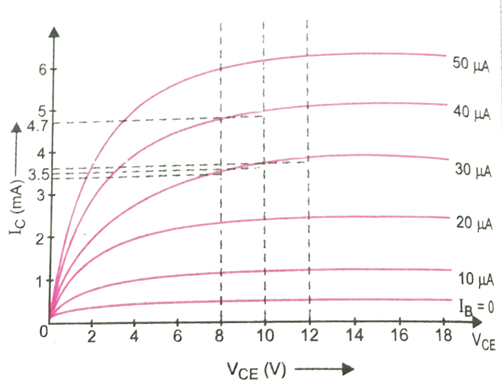
View SolutionOutput characteristics of an n-p-n transistor in CE configuration is shown in the Fig. Determine

(i) dynamic output resistance (ii) dc current gain and (iii) ac current gain at an opererating point VCE=10V, when IB=30μA.
View SolutionDraw the tramsfer characteristic curve of a base biased transistor in CE configuration. Explain clearly how the active region of the Vo versus Vi curve in a transistor is used as an amplifier.
View Solution
