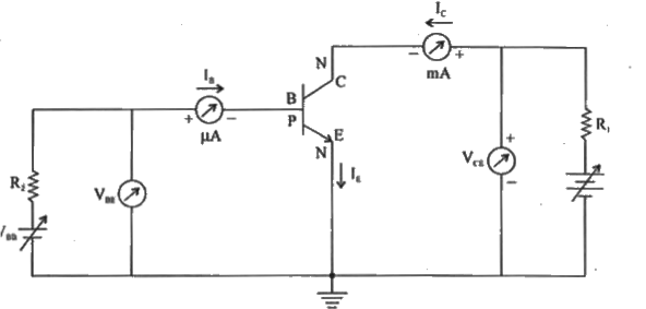
Show the circuit arrangement for studying the input and output characteristics of a n-p-n transistor in CE configuration.Solution in Kannada
Topper's Solved these Questions
- SEMICONDUCTOR ELECTRONICSBOOK - SUBHASH PUBLICATIONCHAPTER - SEMICONDUCTOR ELECTRONICSEXERCISE - FIVE MARKS QUESTIONS WITH ANSWERS
9 Videos
- SEMICONDUCTOR ELECTRONICSBOOK - SUBHASH PUBLICATIONCHAPTER - SEMICONDUCTOR ELECTRONICSEXERCISE - OPTIONAL NUMERICALS WITH SOLUTIONS
6 Videos
- SEMICONDUCTOR ELECTRONICSBOOK - SUBHASH PUBLICATIONCHAPTER - SEMICONDUCTOR ELECTRONICSEXERCISE - OPTIONAL NUMERICALS WITH SOLUTIONS
6 Videos
- RAY OPTICS AND OPTICAL INSTRUMENTSBOOK - SUBHASH PUBLICATIONCHAPTER - RAY OPTICS AND OPTICAL INSTRUMENTSEXERCISE - NUMERICALS WITH SOLUTIONS
22 Videos
- SUPER MODEL QUESTION PAPER ( WITH ANSWERS ) BOOK - SUBHASH PUBLICATIONCHAPTER - SUPER MODEL QUESTION PAPER ( WITH ANSWERS ) EXERCISE - PART D
26 Videos
Similar Questions
What is half wave rectification? Explain the working of a half wave rectifier. Indicate the waveforms of input and output voltage.
View SolutionIf the peak value voltage in the secondary output ac voltage is 12V, then what will be the average DC in the case of HWR and FWR?
View SolutionIf the peak value voltage in the secondary output ac voltage is 12V, then what will be the average DC in the case of HWR and FWR?
View SolutionShow that lateral shift is equal to the thickness of the slab for grazing incidence.
View SolutionDerive an expression for electrical conductivity.
View SolutionWhich is correct for the graph ?

View SolutionDraw a circuit diagram of a CE amplifier by using n-p-n transistor and show input and output voltages graphically.
View SolutionDraw typical output characteristics of an n-p-n transistor in CE configuration. Show how these characteristics can be used to determine output resistance.
View SolutionDraw the typical input and output characteristics of an n-p-n transistor in CE configuration. Show how these characteristics can be used to determine (a) the input resistance (ri) and (b) current amplification factor (β).
View SolutionOutline the method of drawing input and output characteristics with a neat labelled diagram of an N-P-N transistor in CE configuration.
View SolutionDraw circuit diagram for n-p-n transistor to draw input and output characteristics in common base configuration. Draw the input and ouput curves and explain them.
View SolutionDraw a circuit diagram to study characteristics of n-p-n transistor in CE configuration. Draw the sketch of input and output characteristics of this configuration . Define current amplification factor ?
View SolutionWhat is amplification? With a circuit diagram, explain the working of npn transistor as an amplifier in CE configuration.
View Solution(i) Draw a circuit diagram to study the input and output characteristics of an n-p-n transistor in its common emitter configuration. Draw the typical input and output characteristics.
(ii) Explain, with the hepl of a circuit diagram, the working of n-p-n transistor as a common emitter amplifier.
View Solution(a) Draw the circuit arrangement for studying the input and output characteristics of an n-p-n transistor in CE configuration . With the help of these characteristics define (i) input resistance , (ii) current amplification factor . (b) Describe briefly with the help of a circuit diagram how an n-p-n transistor is used to produce self-sustained oscillations .
View Solution

