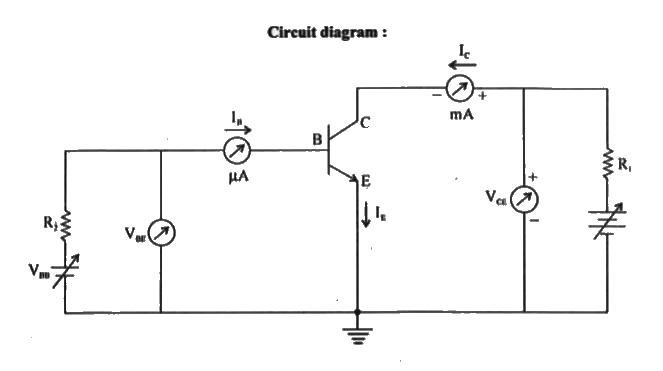
Outline the method of drawing input and output characteristics with a neat labelled diagram of an N-P-N transistor in CE configuration. Solution in Kannada
Input characteristics:
i. The voltage across the collector and emitter is maintained constant, say (VCE≥5V)
ii. The VBB is varied and the corresponding VBEandIB(μA) are tabulated.
iii. A graph of IB along the y - axis and VBE along the x-axis is plotted. this graph is known as input characteristic curve.
iv. The straight line portion with a constant slope is considered to calculate static as well as dynamic inpute resistance.
ri=(ΔVBEΔIB)VCE→ Dynamic resistance and ri=(VBEIB)VCE→ Static resistance
Output characteristics :
i. The voltage VBB is adjusted for a suitable base current (say 10 μA to 60 μA).
ii. The voltage across VCE is varied by varying VCC and the corresponding collector current IC is noted.
iii. The results are tabulated.
iv. A graph of IC (mA) along the y-axis and VCE (volts ) along the x -axis is plotted.
v. The curve obtained is called output characteristics.
vi. The output resistance 'r0'is calculated by using the formula r0=(ΔVCEΔIC)Ip
Note: the ratio(ΔICΔIB)VCE is known as current amplification factor (β)

Topper's Solved these Questions
- SEMICONDUCTOR ELECTRONICSBook:SUBHASH PUBLICATIONChapter:SEMICONDUCTOR ELECTRONICSExercise:OPTIONAL NUMERICALS WITH SOLUTIONS
Explore 6 Videos
- SEMICONDUCTOR ELECTRONICSBook:SUBHASH PUBLICATIONChapter:SEMICONDUCTOR ELECTRONICSExercise:TWO MARKS QUESTIONS WITH ANSWERS
Explore 42 Videos
- RAY OPTICS AND OPTICAL INSTRUMENTSBook:SUBHASH PUBLICATIONChapter:RAY OPTICS AND OPTICAL INSTRUMENTSExercise:NUMERICALS WITH SOLUTIONS
Explore 22 Videos
- SUPER MODEL QUESTION PAPER ( WITH ANSWERS ) Book:SUBHASH PUBLICATIONChapter:SUPER MODEL QUESTION PAPER ( WITH ANSWERS ) Exercise:PART D
Explore 26 Videos
Similar Questions
If the peak value voltage in the secondary output ac voltage is 12V, then what will be the average DC in the case of HWR and FWR?
View SolutionRepresent a NOT gate using a NAND gate or a NOR gate.
View SolutionShow that lateral shift is equal to the thickness of the slab for grazing incidence.
View SolutionDerive an expression for electrical conductivity.
View SolutionWhich is correct for the graph ?

View SolutionDraw the circuit diagram for studying the characteristics of a transistor in common emitter configuration. Explain briefly and show how input and output characteristics are drawn.
View SolutionDraw a circuit diagram of a CE amplifier by using n-p-n transistor and show input and output voltages graphically.
View SolutionDraw typical output characteristics of an n-p-n transistor in CE configuration. Show how these characteristics can be used to determine output resistance.
View SolutionShow the circuit arrangement for studying the input and output characteristics of a n-p-n transistor in CE configuration.
View SolutionDraw a circuit diagram to obtain the characteristics of a n-p-n transistor in common base configuration . Give shape of input and output characteristic curves.
View SolutionDraw circuit diagram for n-p-n transistor to draw input and output characteristics in common base configuration. Draw the input and ouput curves and explain them.
View SolutionDraw a circuit diagram to study characteristics of n-p-n transistor in CE configuration. Draw the sketch of input and output characteristics of this configuration . Define current amplification factor ?
View Solution(i) Draw a circuit diagram to study the input and output characteristics of an n-p-n transistor in its common emitter configuration. Draw the typical input and output characteristics.
(ii) Explain, with the hepl of a circuit diagram, the working of n-p-n transistor as a common emitter amplifier.
View Solution(a) Draw the circuit arrangement for studying the input and output characteristics of an n-p-n transistor in CE configuration . With the help of these characteristics define (i) input resistance , (ii) current amplification factor . (b) Describe briefly with the help of a circuit diagram how an n-p-n transistor is used to produce self-sustained oscillations .
View SolutionDraw typical output characteristics of an n-p-n transistor in CE configuration. Show how these characteristics can be used to determine output resistance.
View Solution

