(a) Draw the circuit arrangement for studying the input and output characteristics of an n-p-n transistor in CE configuration . With the help of these characteristics define (i) input resistance , (ii) current amplification factor .
(b) Describe briefly with the help of a circuit diagram how an n-p-n transistor is used to produce self-sustained oscillations .
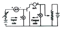
(a) Common emitter (CE) transistor characteristic : The transistor is most widely used in the CE configuration . When a transistor is used in CE configuration , the input is between the base and emitter and the output is between the collector and emitter .
The input and output characteristics of an n-p-n transistor in CE configuration can be studied by using the given circuit .
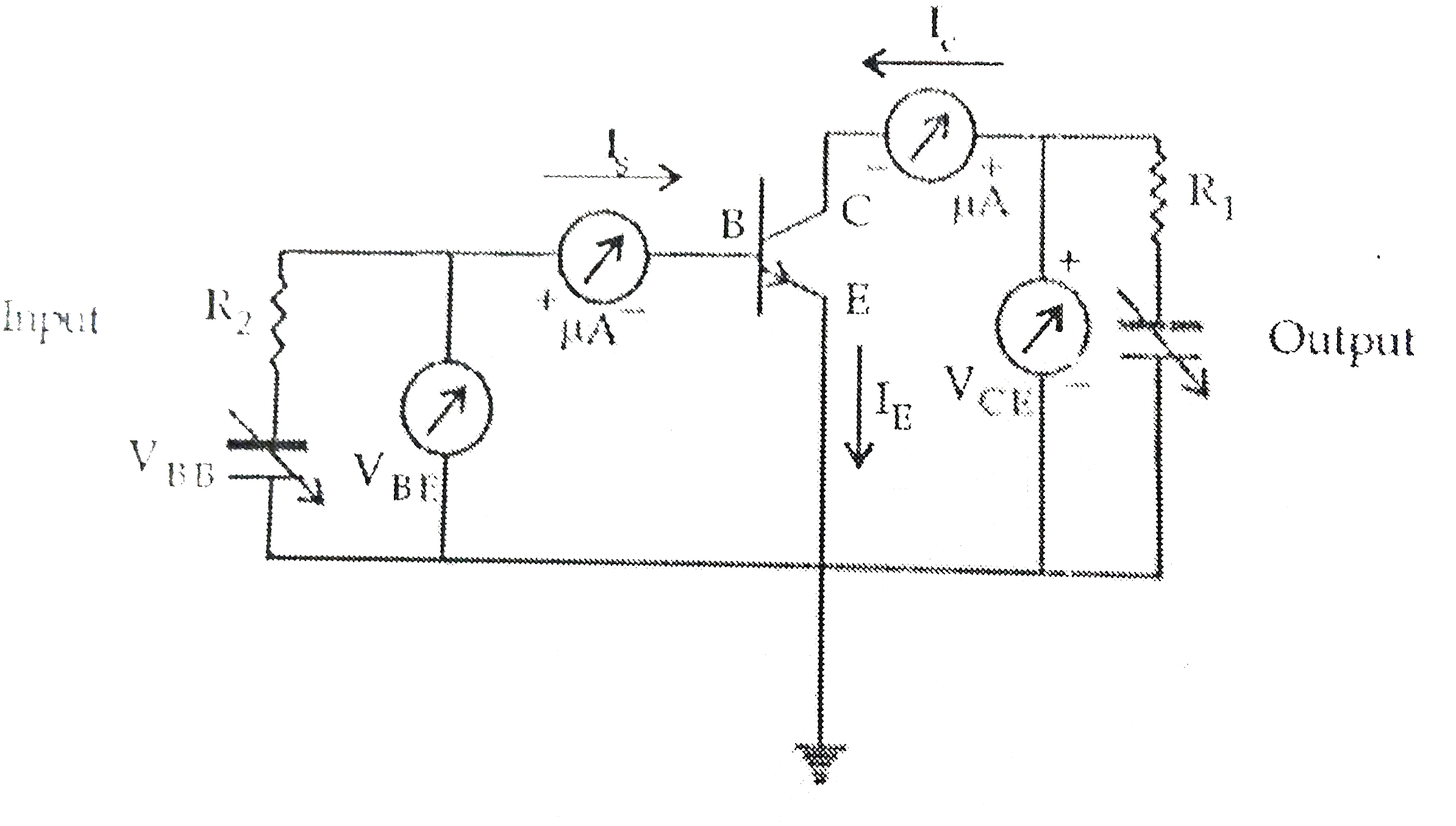
(i) Input characteristics : The variation of the base current IB with the base emitter voltage VBE is called the input characteristics keeping VCE fixed . A curve is plotted between the base current IB against the base emitter voltage VCE is kept fixed .
Since VCE=VCB+VBE and for Silicon (Si) transistor VBE is 0.6 to 0.7 V,VCE must be larger than 0.7 V . The input characteristics of a transistor is shown in fig. (a) .
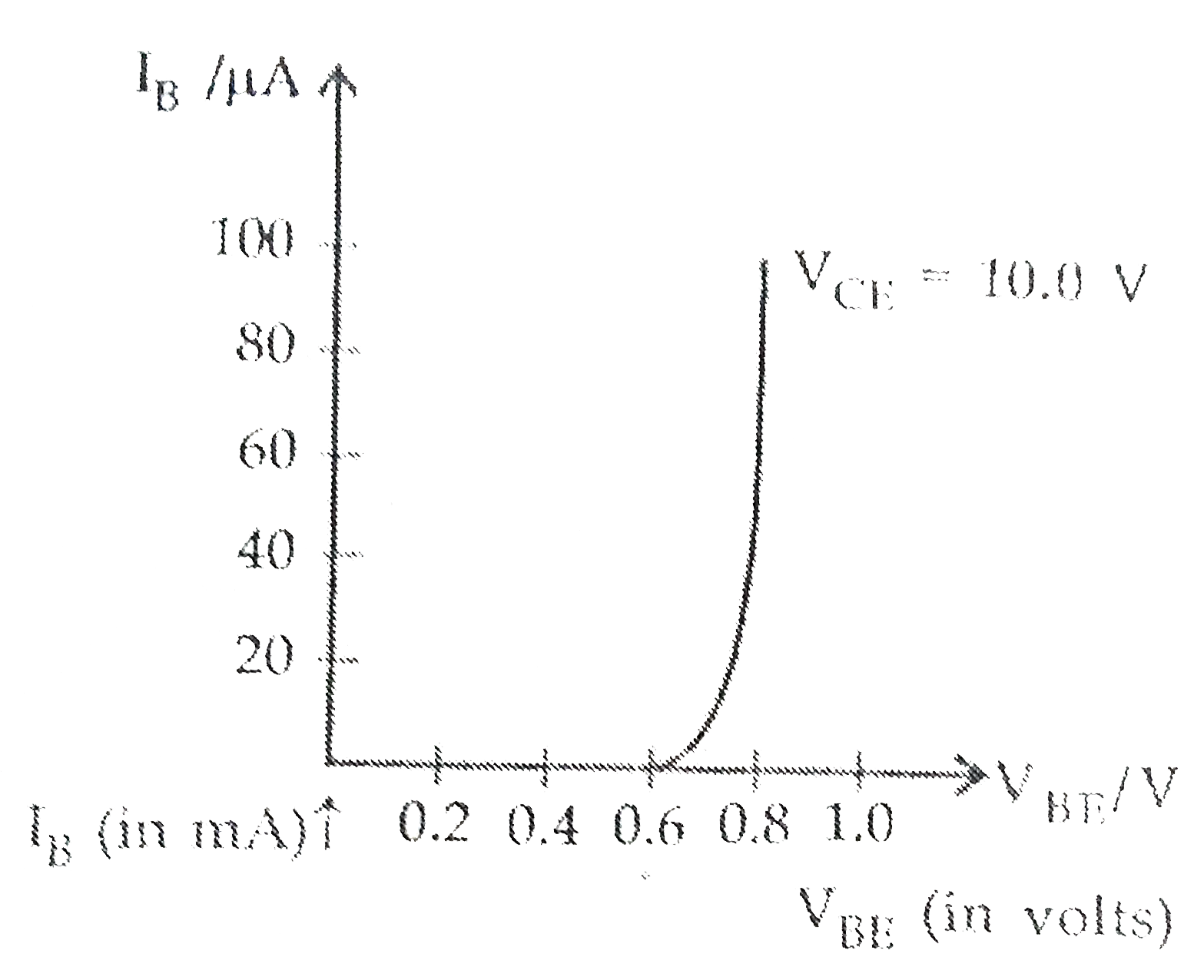
(ii) Output characteristics : The variations of the collector current IC with the collector emitter voltage VCE , keeping the base current IB constant is called output characteristics .
The plot of IC versus VCE for different fixed values of IB gives one output characteristic . The different output characteristics for different values of IB is shown in ltbegt 
(iii) Input Resistance : This is defined as the ratio of the change in collector-emitter voltage (ΔVCE) to the resulting change in base current (ΔIB) at constant collector-emitter voltage (VCE).
∴ ri=(ΔVBEΔIB)VCE
(iv) Output Resistance : This is defined as the ratio of the change in base-emitter voltage (ΔVE) to the change in collector current (ΔIC) at constant base current IB.
∴ r0=(ΔVCEΔIC)IB
(v) Current Amplification Factor (β): This is defined as the ratio of the change in collector current (ΔIC) to change in base current (ΔIB) at constant VCB.
βac=(ΔICΔIB)VCE
This is also known as current gain .
Topper's Solved these Questions
- XII BOARDSBook:XII BOARD PREVIOUS YEAR PAPER ENGLISHChapter:XII BOARDSExercise:SET -II
Explore 9 Videos
- XII BOARDSBook:XII BOARD PREVIOUS YEAR PAPER ENGLISHChapter:XII BOARDSExercise:SET -III
Explore 4 Videos
- XII BOARDSBook:XII BOARD PREVIOUS YEAR PAPER ENGLISHChapter:XII BOARDSExercise:SET-III DELHI BOARD
Explore 10 Videos
- SAMPLE PAPER 2019Book:XII BOARD PREVIOUS YEAR PAPER ENGLISHChapter:SAMPLE PAPER 2019Exercise:SECTION D
Explore 6 Videos
Similar Questions
Draw the typical input and output characterisitics of an n-p-n transistor in CE configurtion . Show how these characteristic can be used to determine (a) the input resistance (r1) and (b) current amplification factor (β).
View SolutionDraw typical output characteristics of an n-p-n transistor in CE configuration. Show how these characteristics can be used to determine output resistance.
View SolutionDraw the diagram of the circuit arangement used for studying the 'input' and the 'output' characteristics of an n-p-n transistor inits CE configuration. Briefly explain how these two types of characteristics are obtained and draw these characteristics.
(b) 'Define' the terms (i) Input resistance, (ii) Output resistance , (iii) Current amplification factor, for a given transistor.
View Solution(i) Draw a circuit diagram to study the input and output characteristics of an n-p-n transistor in its common emitter configuration. Draw the typical input and output characteristics.
(ii) Explain, with the hepl of a circuit diagram, the working of n-p-n transistor as a common emitter amplifier.
View SolutionOutput characteristics of an n-p-n transistor in CE configuration is shown in the Fig. Determine
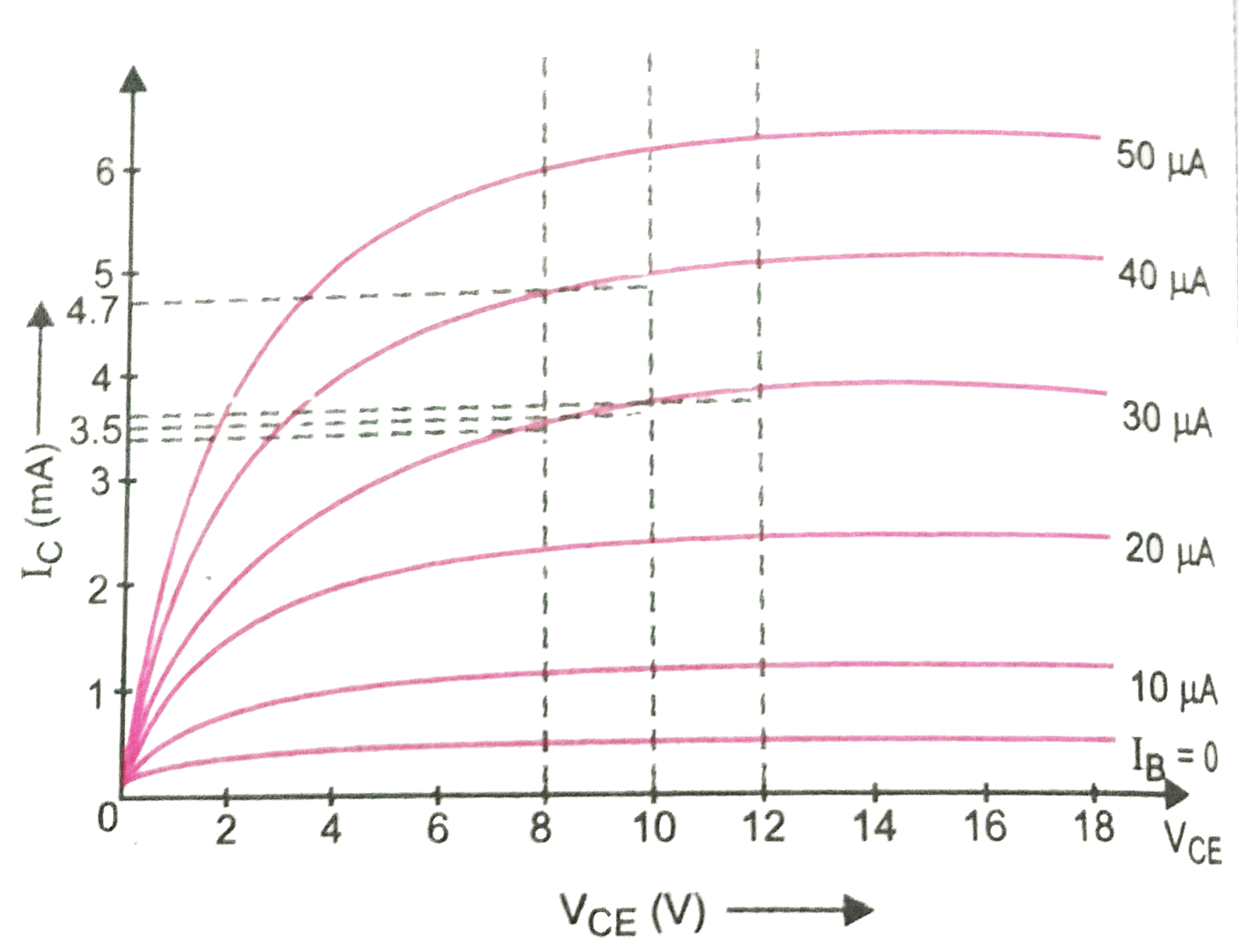
(i) dynamic output resistance (ii) dc current gain and (iii) ac current gain at an opererating point VCE=10V, when IB=30μA.
View Solution(i) Write the functions of three segments of a transistor.
(ii) Draw the ciruit diagram or studying the input and output characteristics of n-p-n transisfor in common emitter configuration . Using the circuit explain how input characteristics are obtained .
View SolutionDescribe briefly the functions of the three segments of n-p-n transistor.
View SolutionExplain with the help of a circuit diagram, the working of a p−n junction diode as a half wave rectifier.
View SolutionConsider the circuit arrangnent shown in Fig. for studying input and output characteristics of npn transistor in CE configuration.
Select the values of R and R for a transistor whose VBE=0.7V, so that the transistor is operating at point Q as shown in the characteristics shown in Fig.
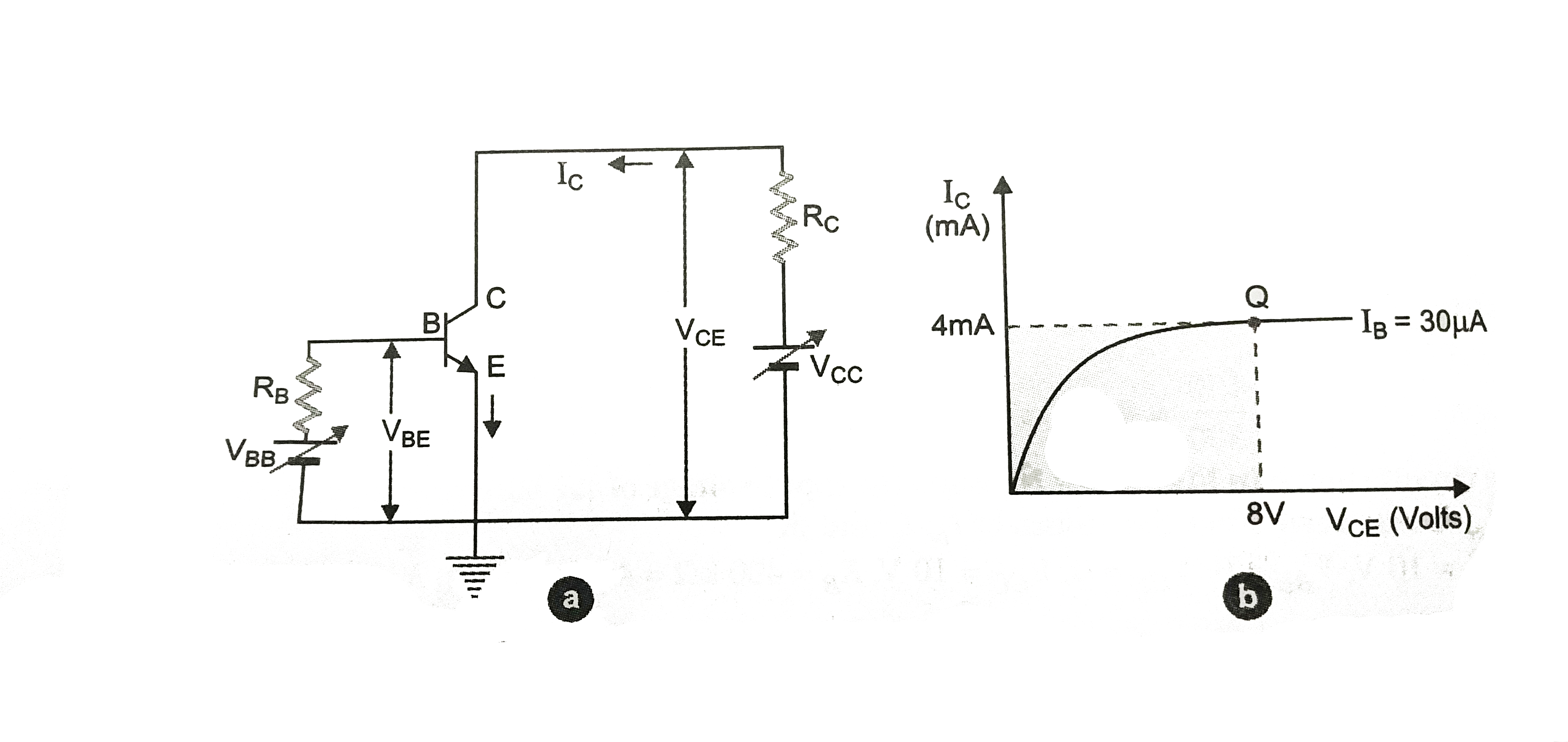 Given that the input impedance of the transistor is very small and VCC=VBB=16V, also find the voltage gain and power gain of circuit making appropriate assumptions.
View SolutionThe circuit diagram below shows n-p-n transistor in CE configuration. For this configuration, mark the correct statement(s).
View Solution

