Complete Solutions to EXERCISE - II of chapter SEMICONDUCTOR DEVICES of Class 12 book with complete answers and questions
| Class 12 | PHYSICS |
| Chapter | SEMICONDUCTOR DEVICES |
| AAKASH SERIES | EXERCISE - II |
| Number Of Questions | 31 |
| Academic Year | 2023-24 |
A full-wave p-n diode rectifier uses a load resistor of `1500Omega`. No filter is used. The forward bias resistance of the diode is `10Omega`. The efficiency of the rectifier is
View SolutionA p-n junction (D) shown in the figure can act as a rectifier. An alternating current source(V) is connected in the circuit. The current (I) in the resistor (R) can be shown by:

View SolutionThe input signal given to a CE amplifier having a voltage gain of 150 is `V_(i) = 2cos(15t+(pi)/(3))` The corresponding output signal will be
View SolutionIn the figure shown, the currents through the series resistance and load resistance are respectively

View SolutionThe value of the resistor, `R_(s)`, needed in the de voltage regulator circuit shown here, equals :

View SolutionThe current gain of a transistor in common base and common-emitter configurations called `alpha and beta` are related as
View SolutionFor a transistor, the value of `alpha= 0.9`, then the value of B is
View SolutionThe current gain in common-base configuration of n-p-n transistor is 0.8. The current amplification factor in common-emitter configuration is
View SolutionFor a transistor, the current gain of common- base configuration is 0.8. If the transistor is in common-emitter configuration and the base current changes by 5mA, then the change in collector current is
View SolutionCalculate the current amplification factor `beta` when change in collector current is 1mA and change in base current is `20muA`.
View SolutionA change of 200mV in base-emitter voltage causes a change of `100muA` in the base current. The input resistance of the transistor is
View SolutionThe emitter current in a transistor is 2.2mA and the collector current is 2mA. The base current is
View SolutionWhile a collector-emitter voltage is constant in a transistor, the collector current changes by 8.2mA when the emitter current changes by 8.3mA. The change in base current is
View SolutionIf in a transistor if `(I_(C))/(I_(E))=alpha` and `(I_(C))/(I_(B))=beta` , If `alpha` varies between `(20)/(21)" and "(100)/(101)`, then the value of `beta` lies between
View SolutionWhich of the following logic gates the given truth table represents
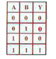
View SolutionWhich of the following logic gates the given truth table represents
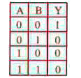
View SolutionThe logic symbol shown in figure represents

View SolutionThe arrangement shown in figure performs the logic function of

View SolutionThe name of the gate obtained by the combination as shown is

View SolutionGiven below are four logic gate symbols. Those for OR, NOR and AND are respectively
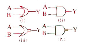
View SolutionIdentify the gate represented by the block diagram is

View SolutionIn Boolean expression which gate is expressed as `y =bar( A+B )`
View SolutionWhat will be the inputs of A and B for Boolean expression `(bar(A + B))+(bar(A.B)) =0` ?
View SolutionIn the given Boolean expression, `Y = A.barB+ B.barA` if A=1, B=1 then Y will be
View SolutionThe logic circuit shown below has the input waveforms 'A' and 'B' as shown. Pick out the current output waveform.

View SolutionIn the circuit below, A and B represent two inputs and C represents the output. The circuit represents
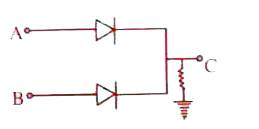
View SolutionThe output (X) of the logic circuit shown in figure will be

View SolutionTo get output 1 for the following circuit, the correct choice for the input is
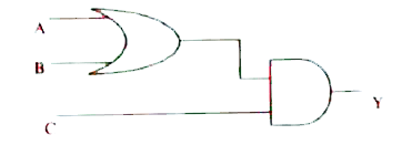
View SolutionThe given electrical network is equivalent to

View SolutionWhich one of the following represents forward bias diode?
View SolutionIn the combination of the following gates the output Y can be written in terms of inputs A and B as
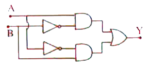
View Solution
EXERCISE - II questions and complete solutions for chapter SEMICONDUCTOR DEVICES of JEE (MAIN AND ADVANCED) PHYSICS of Class 12
All Exercises from AAKASH SERIES Class 12 PHYSICS SEMICONDUCTOR DEVICES
- Example
- EXAMPLES
- Exercise (Long answer questions)
- Exercise (Short answer questions)
- Exercise (very Short answer questions)
- EXERCISE - IA
- EXERCISE - II
- EXERCISE -I (ASSERTION & REASON)
- EXERCISE -I (ENERGY BANDS AND CLASSIFICATION OF SOLIDS )
- EXERCISE -I (LOGIC GATES)
- EXERCISE -I (MATCHING TYPE QUESTIONS)
- EXERCISE -I (MORE THAN ONE OPTION TYPE QUESTIONS)
- EXERCISE -I (P-N JUNCTION DIODE)
- EXERCISE -I (TRANSISTORS)
- EXERCISE -II (ENERGY BANDS AND CLASSIFICATION OF SOLIDS )
- EXERCISE -II (LOGIC GATES)
- EXERCISE -II (P-N JUNCTION DIODE)
- EXERCISE -II (TRANSISTORS )
- PRACTICE EXERCISE (ENERGY BANDS AND CLASSIFICATION OF SOLIDS )
- PRACTICE EXERCISE (LOGIC GATES )
- PRACTICE EXERCISE (TRANSISTORS )
- PROBLEMS
- Problems (LEVEL-I)
- Problems (LEVEL-II)