Complete Solutions to EXERCISE -I (P-N JUNCTION DIODE) of chapter SEMICONDUCTOR DEVICES of Class 12 book with complete answers and questions
| Class 12 | PHYSICS |
| Chapter | SEMICONDUCTOR DEVICES |
| AAKASH SERIES | EXERCISE -I (P-N JUNCTION DIODE) |
| Number Of Questions | 35 |
| Academic Year | 2023-24 |
The neutral region formed at P-n junction due to recombination of electrons and holes is
View SolutionThe potential barrier at a P-n junction is due to the charges on either side of the junction. These charges are
View SolutionIn an unbiased p-n junction, holes diffuse from the p-region ton-region because
(a) free electron in the n-region attract them.
(b ) they move across the junction by the potential difference.
(c ) hole concentration in p-region is more as compared to n-region.
(d ) All the above.
View SolutionOne slab of p type, if physically join to another n type semiconductor, there is no possibility for the formation of pn junction because
View SolutionIf a p-n junction diode is not connected to any circuit,
View SolutionThe electrical resistance of depletion layer is large because
View SolutionIn a PN junction
View SolutionThe barrier potentials for silicon and Germanium diodes are about
View SolutionThe dominant mechanisms for motion of charge carriers in forward and reverse biased silicon p-n junctions are,
View SolutionIn a semi conductor diode, the barrier potential opposes diffusion of
View SolutionThe correct curve between potential and distance near P-N junction is
View SolutionWhen p-n junction diode is forward biased
View SolutionWhich of the following statement is not correct when a junction diode in forward bias?
View SolutionThe resistance of an ideal diode in forward biased condition is
View SolutionThe resistance of an ideal diode in reverse biased condition is
View SolutionIn forward biased condition, the p-n junction diode behaves as
View SolutionReverse bias applied to a junction diode
View SolutionIn the middle of the depletion layer of a reverse biased p-n junction, the
View SolutionAvalanche breakdown in a semiconductor diode occurs when
View SolutionWhen a P-n junction diode is reverse biased the flow of current across the junction is mainly due to
View SolutionThe small currents in reverse biased condition of p-n diode are due to
View SolutionA P-n junction diode can be used as
View SolutionA diode as a rectifier converts
View SolutionIn half-wave rectifier, maximum percentage of A.C. power that can be converted into D.C. power is
View SolutionIn a half-wave rectifier, the load current flows for
View SolutionMaximum efficiency of a full-wave rectifier is
View SolutionIn a full-wave rectifier, the load current flows for
View SolutionZener breakdown occurs
View SolutionAt breakdown region of a Zener diode, which of the following does not change much
View SolutionZener diode can be used
View SolutionIn an unbiased n-p junction electrons diffuse from n-region to p-region because:
View SolutionLEDS are advantageous over conventional incandescent low power lamps.
a) Emitted light is nearly monochromatic b) Less power c) Slow in action
View SolutionThe I - V characterisic of an LED is
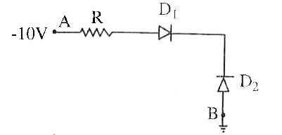
View SolutionIn the figure assuming the diodes to be ideal

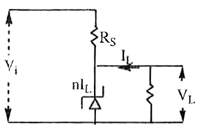
View SolutionThe value of the resistor, `R_s` needed in the dc voltage regulator circuit shown here, equals :

View Solution
EXERCISE -I (P-N JUNCTION DIODE) questions and complete solutions for chapter SEMICONDUCTOR DEVICES of JEE (MAIN AND ADVANCED) PHYSICS of Class 12
All Exercises from AAKASH SERIES Class 12 PHYSICS SEMICONDUCTOR DEVICES
- Example
- EXAMPLES
- Exercise (Long answer questions)
- Exercise (Short answer questions)
- Exercise (very Short answer questions)
- EXERCISE - IA
- EXERCISE - II
- EXERCISE -I (ASSERTION & REASON)
- EXERCISE -I (ENERGY BANDS AND CLASSIFICATION OF SOLIDS )
- EXERCISE -I (LOGIC GATES)
- EXERCISE -I (MATCHING TYPE QUESTIONS)
- EXERCISE -I (MORE THAN ONE OPTION TYPE QUESTIONS)
- EXERCISE -I (P-N JUNCTION DIODE)
- EXERCISE -I (TRANSISTORS)
- EXERCISE -II (ENERGY BANDS AND CLASSIFICATION OF SOLIDS )
- EXERCISE -II (LOGIC GATES)
- EXERCISE -II (P-N JUNCTION DIODE)
- EXERCISE -II (TRANSISTORS )
- PRACTICE EXERCISE (ENERGY BANDS AND CLASSIFICATION OF SOLIDS )
- PRACTICE EXERCISE (LOGIC GATES )
- PRACTICE EXERCISE (TRANSISTORS )
- PROBLEMS
- Problems (LEVEL-I)
- Problems (LEVEL-II)