Complete Solutions to EXAMPLES of chapter SEMICONDUCTOR DEVICES of Class 12 book with complete answers and questions
| Class 12 | PHYSICS |
| Chapter | SEMICONDUCTOR DEVICES |
| AAKASH SERIES | EXAMPLES |
| Number Of Questions | 56 |
| Academic Year | 2023-24 |
The energy of a photon of sodium light `( lamda = 589 nm)` equal to the band gap of a semiconducing material .
Find the minimum energy E required to create a hole -electron pair.
View SolutionThe energy of a photon of sodium light `( lamda = 589 nm)` equal to the band gap of a semiconducing material .
Find the value of E /kT at a temperature of 300 K.
View SolutionPure Si at 300 K has equal electron `(n_(e))` and hole `(n_(h))` concentration of `1.5xx10^(16) m^(-3)` . Doping by indium increases `n_(h)` to `4.5xx10^(22)m^(-3)` . Calculate `n_(e)` in the doped silicon.
View SolutionSuppose a pure Si crystal has `5 xx 10^(28)` atoms `m^(-3)`. It is doped by 1 ppm concentration of pentavalent As. Calculate the number of electrons and holes. Given that `n_(i) = 1.5 xx 10^(16) m^(-3)`.
View SolutionA semiconductor has an electron concentration of `0.45 xx 10^(12) m^(-3)` and a hole concentration of `5.0 xx 10^(20) m^(-3)` Calculate its conductivity. Given electron mobility `=0.135 m^2 V^(-1) s^(-1)` , hole mobility` =0.048m^2 V^(-1) s^(-1) `
View SolutionAn N-type silicon sample of width `4 xx10^(-3)` m thickness 0.25mm and length `6 xx 10^(-2)` m carries a current of 4.8 mA when the voltage is applied across the length of the sample. What is the current density? If the free electron density is `10^(22) m^(-3)` , then find how much time it takes for the electrons to travel the full length of the sample.
View SolutionThe V-I characteristic of a silicon diode is shown in the Fig. Calculate the resistance of the diode at
`I_D =15 mA `
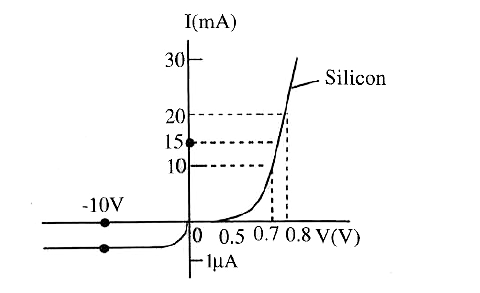
View SolutionThe V-I characteristic of a silicon diode is shown in the Fig. Calculate the resistance of the diode at
`V_D =- 10 V`
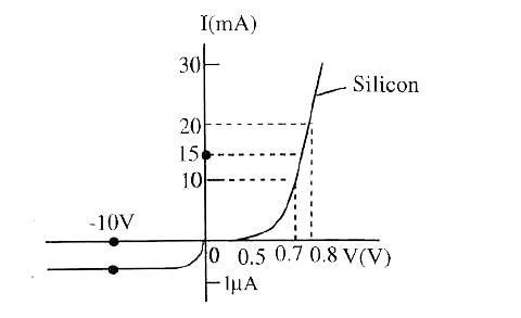
View SolutionFind maximum voltage across AB in the circuit shown in figure. Assume that the diode is ideal.
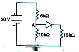
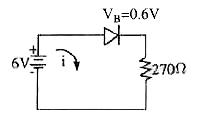
View SolutionIn the given circuit diagram. `V_B ~~0.6V`
Calculate the current i in the circuit.
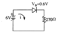
View SolutionIn the given circuit diagram. `V_B ~~0.6V`
Find the current (I) if the diode is reversed.
View SolutionIn a p-n junction diode, the depletion region is 400 nm wide and an electric field of `5 xx 10^5 V//m` exists in it. The minimum kinetic energy of a conduction electron which can diffuse from n side to p side is
View SolutionTwo junction diodes, one of germanium (Ge) and other of silicon (Si) are connected as shown in fig to a battery of 12V and a load resistance `10 k Omega `. The germanium diode conducts at 0.3V and silicon diode at 0.7V. When current flows in the circuit, the potential of terminal Y will be
` (##AKS_NEO_CAO_PHY_XII_V02_C_C06_SLV_013_Q01.png" width="80%">
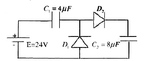
View SolutionIn the circuit shown, the potential drop across each capacitor is (assuming the two diodes are ideal)
View SolutionA potential barrier of 0.50 V exists across a p-n junction.
If the depletion region is `5.0 xx 10^(-7) ` m wide, what is the intensity of the electric field in this region ?
View SolutionA potential barrier of 0.50 V exists across a p-n junction.
An electron with a speed of `5.0 xx 10^5 ` m/s approaches the p-n junction from the n-side. With what speed will it enter the p-side ?
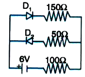
View SolutionThe circuit shown below contains two diodes, each of forward resistance, 50 `Omega` and with infinite backward resistance. If the battery voltage is 6V, find the current through 100 `Omega` resistance.
View SolutionThe applied input ac power to a half wave rectifier is 100 W. The dc output power obtained is 40W. Find the rectifier efficiency.
View SolutionA p-n diode is used in a half wave rectifier with a load resistance of `1000 Omega `. If the forward resistance (`r_f`) of diode is `10 Omega `, calculate the efficiency of this half wave rectifier.
View SolutionA full wave rectifier uses two diodes with a load resistance of `100 Omega `. Each diode is having negligible forward resistance. Find the efficiency of this full wave rectifier
View SolutionThe current through a P-N junction diode is 55mA at a forward bias voltage of 3.0 V. If the temperature is `27^@ C`, find the static resistance of the diode.
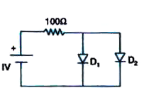
View SolutionConsidering the circuit and data given in the diagram calculate the currents flowing in the diodes `D_(1)` and `D_(2)` with linear characteristics.Forward resistance of `D_(1)` and `D_(2)` is 20 `Omega`
View SolutionIf a p-n junction diode, a square input signal of 10V is applied as shown,
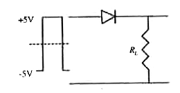
then the output signal across `R_L` will be

View SolutionFor the circuit shown in Fig. find
the output voltage,
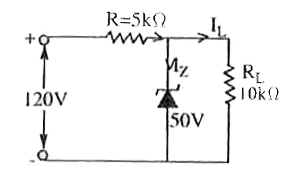
View SolutionFor the circuit shown in Fig. find
the voltage drop across series resistance,
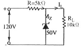
View SolutionFor the circuit shown in Fig. find
the current through Zener diode.
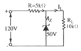
View SolutionA zener diode has a breakdown voltage of 9.1 volts with a maximum power dissipation of 364 milliwatts. What is the maximum current the diode can handle?
View SolutionIn a single state transistor amplifier, when the signal changes by 0.02 V, the base current change by 10uA and collector current by ` 10 mu `A. If collector load `R_c = 2k Omega and R_L = 10k Omega `, Calculate :
Current Gain
View SolutionIn a single state transistor amplifier, when the signal changes by 0.02 V, the base current change by 10uA and collector current by ` 10 mu `A. If collector load `R_c = 2k Omega and R_L = 10k Omega `, Calculate :
Input impedance,
View SolutionIn a single state transistor amplifier, when the signal changes by 0.02 V, the base current change by 10uA and collector current by ` 10 mu `A. If collector load `R_c = 2k Omega and R_L = 10k Omega `, Calculate :
Effective ac load,
View SolutionIn a single state transistor amplifier, when the signal changes by 0.02 V, the base current change by 10uA and collector current by ` 10 mu `A. If collector load `R_c = 2k Omega and R_L = 10k Omega `, Calculate :
Voltage gain and
View SolutionIn a single state transistor amplifier, when the signal changes by 0.02 V, the base current change by 10uA and collector current by ` 10 mu `A. If collector load `R_c = 2k Omega and R_L = 10k Omega `, Calculate :
Power gain.
View SolutionA p-n-p transistor is used in common-emitter mode in an amplifier circuit. A change of `40 mu A` in the base current brings a change of 2 mA in collector current and 0.04 V in base-emitter voltage. Find the : (i) input resistance (`R_("in")`) and (ii) the base current amplification factor (`beta `).
If a load of `6k Omega ` is used, then also find the voltage gain of the amplifier.
View SolutionFor a transistor `beta = 40 and I_B = 25 mu A I_B = 25 mu A.` Find the value of `l_E `.
View SolutionIn a transistor `beta = 45`, the change in the v voltage across `5 k Omega ` resistor which is connected in collector M circuit is 5V. Find the change in base current.
View SolutionCurrent amplification factor of a common base configuration is 0.88. Find the value of base current when the emitter current is 1 mA.
View SolutionIn a transistor, the emitter circuit resistance is `100 kOmega ` and the collector resistance is `100 Omega `. The power gain, if the emitter and collector currents are assumed to be equal, will be
View SolutionIn the following common-emitter configuration an n-p-n transistor with `beta = 100` is used. The output voltage of the amplifier will be
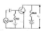
View SolutionAn n-p-n transistor in a common emitter mode is used as a simple voltage amplifier with a collector current of 4 mA. The terminal of a 8 V battery is connected to the collector through a load resistance `R_L` and to the base through a resistance `R_B` The collector-emitter voltage `V_(CE) = 4 V`, base-emitter voltage `V_(BE) = 0.6 V `and base current amplification factor `B_(d.c)` = 100. Calculate the values of `R_L` and `R_B`
View SolutionThe overall gain of a multistage amplifier is 100. When negative feedback is applied, the gain reduces to v 10. Find the fraction of the output that is feedback to the M input.
View SolutionCalculate the gain of
a positive feedback amplifier
View SolutionCalculate the gain of
a negative feedback amplifier with an internal gain of A = 100 and feedback factor `beta =(1)/(1000)`
View SolutionIn a negative feedback amplifier, the gain without feedback is 100, feed back ratio is 1/25 and input voltage is 50 mV. Calculate
gain with feedback
View SolutionIn a negative feedback amplifier, the gain without feedback is 100, feed back ratio is 1/25 and input voltage is 50 mV. Calculate
feedback factor
View SolutionIn a negative feedback amplifier, the gain without feedback is 100, feed back ratio is 1/25 and input voltage is 50 mV. Calculate
output voltage
View SolutionIn a negative feedback amplifier, the gain without feedback is 100, feed back ratio is 1/25 and input voltage is 50 mV. Calculate
feedback voltage
View SolutionIn a negative feedback amplifier, the gain without feedback is 100, feed back ratio is 1/25 and input voltage is 50 mV. Calculate
new input voltage so that output voltage with feedback equals the output voltage without feedback
View SolutionThe Boolean expression of the output Y of the inputs A and B for the circuit shown in the fig
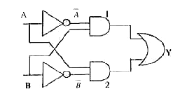
View SolutionThe combination of NAND gates shown here under are equivalent to

View SolutionThe diagram of a logic circuit is given below. The output of the circuit is represented by
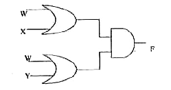
View SolutionThe logic circuit and its truth table are given, what is the gate X in the diagram
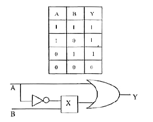
View SolutionDraw the logic circuit corresponding to the Boolean expression. `Y=AB+barBC`.
View SolutionSimplify `Y = AB+ABC +barAB+ AbarBC` using Boolean Algebra. Draw the resultant simplified logic circuit.
View SolutionWrite Boolean equation for the output of fig. and solve this equation for all possible input conditions.

View SolutionDraw logic diagrams for the Boolean expressions given below.
`A * barB + barA * B=Y`
View SolutionDraw logic diagrams for the Boolean expressions given below.
(i)`A . barB+barA . B=Y` , (ii)`(A+barB). (barA+B)=Y`
View Solution
EXAMPLES questions and complete solutions for chapter SEMICONDUCTOR DEVICES of JEE (MAIN AND ADVANCED) PHYSICS of Class 12
All Exercises from AAKASH SERIES Class 12 PHYSICS SEMICONDUCTOR DEVICES
- Example
- EXAMPLES
- Exercise (Long answer questions)
- Exercise (Short answer questions)
- Exercise (very Short answer questions)
- EXERCISE - IA
- EXERCISE - II
- EXERCISE -I (ASSERTION & REASON)
- EXERCISE -I (ENERGY BANDS AND CLASSIFICATION OF SOLIDS )
- EXERCISE -I (LOGIC GATES)
- EXERCISE -I (MATCHING TYPE QUESTIONS)
- EXERCISE -I (MORE THAN ONE OPTION TYPE QUESTIONS)
- EXERCISE -I (P-N JUNCTION DIODE)
- EXERCISE -I (TRANSISTORS)
- EXERCISE -II (ENERGY BANDS AND CLASSIFICATION OF SOLIDS )
- EXERCISE -II (LOGIC GATES)
- EXERCISE -II (P-N JUNCTION DIODE)
- EXERCISE -II (TRANSISTORS )
- PRACTICE EXERCISE (ENERGY BANDS AND CLASSIFICATION OF SOLIDS )
- PRACTICE EXERCISE (LOGIC GATES )
- PRACTICE EXERCISE (TRANSISTORS )
- PROBLEMS
- Problems (LEVEL-I)
- Problems (LEVEL-II)