How p-n junction diode is formed ? And explain depletion layer and barrier potential. Solution in Gujrati
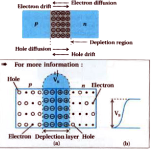
When in one region of Si wafer acceptor impurity (Al) is added the p-type semiconductor and another region donor impurity (As) is added the n-type semiconductor is form. Thus, p-n junction is formed and there is metallic junction between p and n region.
Important processes occur during the formation of a p-n junction. Thus, is diffusion and drift.
The number of electrons or holes per unit volume is called number density of electron or holes.
During formation of p-n junction difference in number densities of p and n semiconductor diffusion of hole takes place from p-semiconductor to n-semiconductor (p→n) and diffusion of electron takes place from n-semiconductor to p-semiconductor (n→p).
This motion of charge carriers gives rise to diffusion current across the junction.
When an electron diffuses from n→p it leaves behind an ionised donor on n-side. This ionised donor (positive charge) is immobile as it is bonded to the surrounding atoms.
As the electrons continue to diffuse from n→p, a layer of positive charge (or positive space charge region) on n-side of the junction is developed.
Similarly, when a hole diffuses from p→n due to the concentration gradient, it leaves behind an ionised acceptor (negative charge) which is immobile.
These ionized charges are immobile means they cannot move.
The space-charge region on either side of the junction together is known as deplection region or depletion layer.
The n-region of depletion layer does not have majority charge carrier electron and in p-region does not have charge carrier holes. These regions are empty in terms of their majority charge carriers.

The thickness of region is of the order of one-tenth of a micrometer in p-n junction. (Means approximately 0.5 μm).
Due to the positive space-charge region on n-side of the junction and negative space charge region on p-side of the junction an electric field directed from positive charge towards negative charge develops. Due to this field, an electron on p-side of the junction moves to n-side and a hole on n-side of the junction moves to p-side. The motion of charge carriers due to the electric field is called drift.
Initially, diffusion current is large and drift current is small.
As the diffusion process continues, the space charge regions on either side of the junction extend thus increasing the electric field strength and hence drift current.
This process continues until the diffusion current equals the drift current.
Thus a p-n junction is formed. Since p-n junction has two connection terminals, it is called p-n junction diode.
In p-n junction under equilibrium there is no net current.
Topper's Solved these Questions
- SEMICONDUCTOR ELECTRONICS : MATERIALS, DEVICES AND SIMPLE CIRCUITS Book:KUMAR PRAKASHANChapter:SEMICONDUCTOR ELECTRONICS : MATERIALS, DEVICES AND SIMPLE CIRCUITS Exercise:Section-B : Numericals (Numerical From Textual illustrations)
Explore 16 Videos
- SEMICONDUCTOR ELECTRONICS : MATERIALS, DEVICES AND SIMPLE CIRCUITS Book:KUMAR PRAKASHANChapter:SEMICONDUCTOR ELECTRONICS : MATERIALS, DEVICES AND SIMPLE CIRCUITS Exercise:Section-B : Numericals (Numerical From Textual Exercise)
Explore 15 Videos
- SEMICONDUCTOR ELECTRONICS : MATERIALS, DEVICES AND SIMPLE CIRCUITS Book:KUMAR PRAKASHANChapter:SEMICONDUCTOR ELECTRONICS : MATERIALS, DEVICES AND SIMPLE CIRCUITS Exercise:Section-D : Multiple Choice Questions (MCQs) (MCQs asked in Competitive Exams)
Explore 129 Videos
- SAMPLE QUESTION PAPER Book:KUMAR PRAKASHANChapter:SAMPLE QUESTION PAPER Exercise:PART-B SECTION-C
Explore 5 Videos
- WAVE OPTICSBook:KUMAR PRAKASHANChapter:WAVE OPTICSExercise:SECTION-D (MULTIPLCE CHOICE QUESTIONS (MCQS)) (MCQS FROM DARPAN BASED ON TEXTBOOK)
Explore 239 Videos
Similar Questions
C, Si and Ge have same lattice structure. Why is C insulator while Si and Ge intrinsic semiconductors?
View SolutionIn an n type silicon, which of the following statements is true:
View SolutionAt absolute zero temperature Si acts as ……..
View SolutionTwo charges –q and +q are located at points (0, 0, –a) and (0, 0, a), respectively.
(a) What is the electrostatic potential at the points (0, 0, z) and (x, y, 0) ?
(b) Obtain the dependence of potential on the distance r of a point from the origin when r/a>>1 .
(c) How much work is done in moving a small test charge from the point (5,0,0) to (–7,0,0) along the x-axis? Does the answer change if the path of the test charge between the same points is not along the x-axis?
View SolutionAccording to particle theory of light what is the velocity of light in a dense medium, compared to that in rare medium ?
View SolutionExplain the term depletion region and potential barrier for a p-n junction.
View SolutionIn a forward biased p-n junction diode, the potential barrier in the depletion region will be of the form
View SolutionHow is a potential barrier formed in p-n junction diode ?
View SolutionExplain the terms 'depletion layer' and 'potential barrier' in a p-n junction diode. How are the (a) width of depletion layer, and (b) value of potential barrier affected when the p-n junction is forward biased ?
View SolutionExplain with the help of a diagram the formation of depletion layer and potential barrier in a p-n junction.
View SolutionExplain with the help of a diagram, how a depletion layer and barrier potential are formed in a junction diode.
View SolutionExplain how the depletion layer and barrier potential are formed in pn junction diode ?
View SolutionIn a p-n junction diode made with Ge, the thickness of depletion layer is 2xx10^(-6) m and barrier potential is 0.3V. Find the strength of the electric field at the junction.
View SolutionIn a p-n junction diode the thickness of depletion layer is 2×10⁻⁶m and barrier potential is 0.3 V. The intensity of the electric field at the junction is :
View SolutionBarrier potential of a p-n junction diode is in dependent on
View Solution