Write short note on zener diode. Solution in Gujrati
Zener diode is a special purpose semiconductor diode, named after its inventor C. Zener.
The symbol for zener diode is as below.

Zener diode is fabricated by heavily doping both p and n-side of junction. Due to this depletion region formed is very thin (<10−6m) and the electric field of the junction is extremely high (~5×10⁶Vm) even for a small reverse bias voltage about 5V.
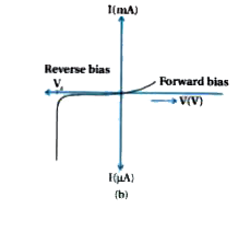
The I→V characteristics of a zener diode is shown in figure (b).

It is seen that when the applied reverse bias voltage (V), reaches the breakdown voltage (VZ) of the zener diode, there is a large change in the current.
Note that after the breakdown voltage VZ, a large change in the current can be produced by almost insignificant change in the reverse bias voltage. So zener voltage remains constant.
This property of the zener diode is used for regulating supply voltages so that they are constant.
We know that reverse current is due to the flow of electrons (minority carriers) from p→n and holes from n→p.
When the reverse bias voltage V becomes to (VZ), then the electric field strength is high enough to pull valence electrons from the host atoms Si or Ge on the p-side which are accelerated to n-side.
These electrons provide a high current during breakdown.
The emission of electrons from the host atoms due to the high electric field is known as internal field emission or field ionisation. The electric field required for field ionisation is of the order of 106V/m.
Topper's Solved these Questions
- SEMICONDUCTOR ELECTRONICS : MATERIALS, DEVICES AND SIMPLE CIRCUITS Book:KUMAR PRAKASHANChapter:SEMICONDUCTOR ELECTRONICS : MATERIALS, DEVICES AND SIMPLE CIRCUITS Exercise:Section-B : Numericals (Numerical From Textual illustrations)
Explore 16 Videos
- SEMICONDUCTOR ELECTRONICS : MATERIALS, DEVICES AND SIMPLE CIRCUITS Book:KUMAR PRAKASHANChapter:SEMICONDUCTOR ELECTRONICS : MATERIALS, DEVICES AND SIMPLE CIRCUITS Exercise:Section-B : Numericals (Numerical From Textual Exercise)
Explore 15 Videos
- SEMICONDUCTOR ELECTRONICS : MATERIALS, DEVICES AND SIMPLE CIRCUITS Book:KUMAR PRAKASHANChapter:SEMICONDUCTOR ELECTRONICS : MATERIALS, DEVICES AND SIMPLE CIRCUITS Exercise:Section-D : Multiple Choice Questions (MCQs) (MCQs asked in Competitive Exams)
Explore 129 Videos
- SAMPLE QUESTION PAPER Book:KUMAR PRAKASHANChapter:SAMPLE QUESTION PAPER Exercise:PART-B SECTION-C
Explore 5 Videos
- WAVE OPTICSBook:KUMAR PRAKASHANChapter:WAVE OPTICSExercise:SECTION-D (MULTIPLCE CHOICE QUESTIONS (MCQS)) (MCQS FROM DARPAN BASED ON TEXTBOOK)
Explore 239 Videos
Similar Questions
C, Si and Ge have same lattice structure. Why is C insulator while Si and Ge intrinsic semiconductors?
View SolutionIn an n type silicon, which of the following statements is true:
View SolutionAt absolute zero temperature Si acts as ……..
View SolutionTwo charges –q and +q are located at points (0, 0, –a) and (0, 0, a), respectively.
(a) What is the electrostatic potential at the points (0, 0, z) and (x, y, 0) ?
(b) Obtain the dependence of potential on the distance r of a point from the origin when r/a>>1 .
(c) How much work is done in moving a small test charge from the point (5,0,0) to (–7,0,0) along the x-axis? Does the answer change if the path of the test charge between the same points is not along the x-axis?
View SolutionAccording to particle theory of light what is the velocity of light in a dense medium, compared to that in rare medium ?
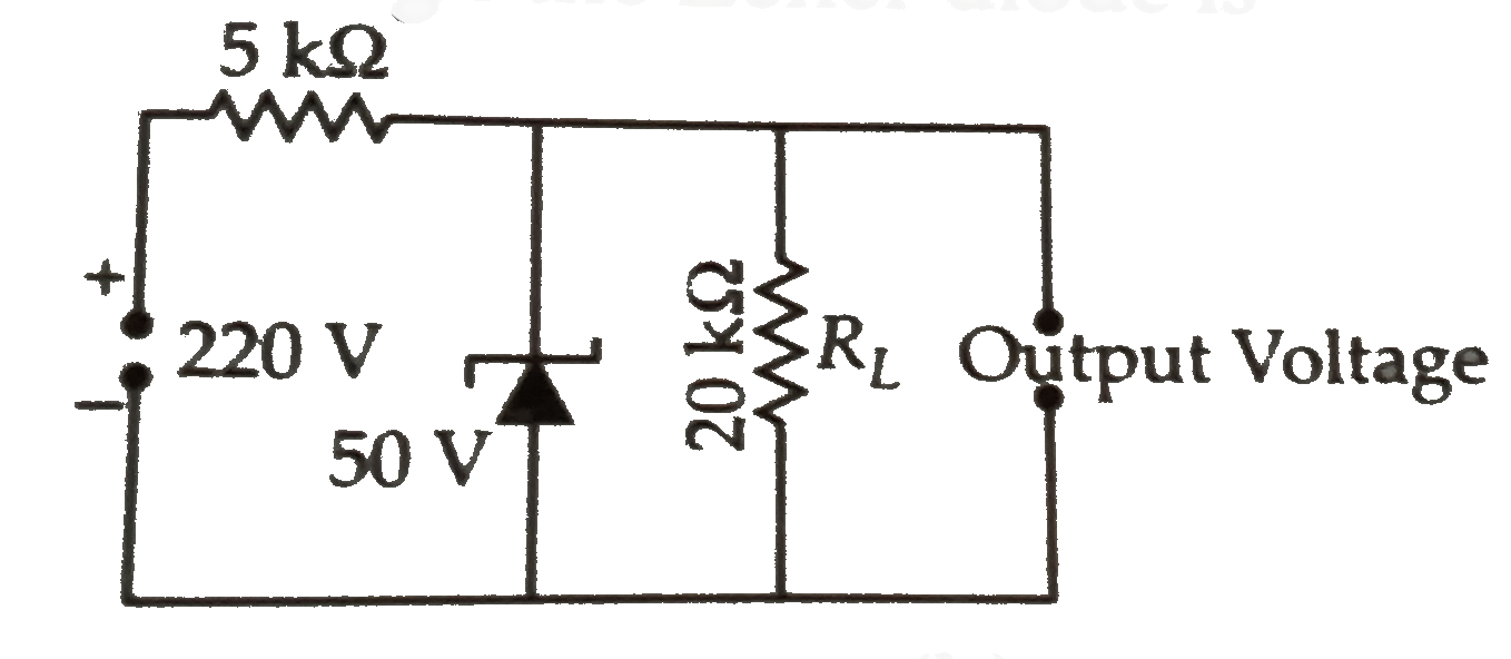
View SolutionFrom the Zener diode circuit shown in figure, the current through the Zener diode is

View Solutionजेनर डायोड का मुख्य उपयोग लिखिए।
View SolutionA Zener diode
View Solutionजेनर डायोड क्या है ? इसका एक उपयोग लिखिए।
View SolutionZener Breakdown | Zener diode and zener diode as voltage regulator
View SolutionWrite the symbol for a zener diode.
View SolutionWrite one important application of zener diode .
View SolutionZener diodes are :
View SolutionWrite down the applications of zener diode.
View SolutionIn a zener diode
View Solution

