When is the p-n junction called reverse bias and explain the change in p-n junction from this type of connection. Solution in Gujrati
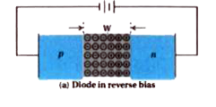
When and external voltage (V) is applied across the diode such that n-side is positive and p-side is negative it is said to be reverse biased. This is shown in figure.

Diagram (b) for the circuit is as follows :

The applied voltage mostly drops across the depletion region according to figure (a).
The direction of applied voltage V0 is same as the direction of barrier potential V. As a result, the barrier height increases and the depletion region widens due to the change in the electric field.

The effective barrier height under reverse bias is V+V0.
In figure (c ), the battery is not connected to p-n junction, potential barrier V0 is shown as 1 and when voltage of the external battery is applied, its effective potential barrier V0+V is shown as 2.
This suppresses the flow of electrons from n→p and holes from p→n due to effective depletion barrier potential means current are disputed due to majority charge carriers hence diffusion current is not obtained.
Although some minority charge carriers pass through the junction due to the high voltage applied by external battery hole in n-region and electron in p-region and current flow in reverse direction is called reverse current. However, for large reverse voltage, the increase in reverse current shows less.
Reverse current does nto depend only on the applied voltage. The current is not limited by the magnitude of the applied voltage but is limited due to the concentration of the minority carrier on either side of junction.
Some voltage is also sufficient to across the junction for minority carriers.
The reverse bias voltage varies from about 10 V to 15 V.
Here current obtained in the order of microampere (μA).
Topper's Solved these Questions
- SEMICONDUCTOR ELECTRONICS : MATERIALS, DEVICES AND SIMPLE CIRCUITS Book:KUMAR PRAKASHANChapter:SEMICONDUCTOR ELECTRONICS : MATERIALS, DEVICES AND SIMPLE CIRCUITS Exercise:Section-B : Numericals (Numerical From Textual illustrations)
Explore 16 Videos
- SEMICONDUCTOR ELECTRONICS : MATERIALS, DEVICES AND SIMPLE CIRCUITS Book:KUMAR PRAKASHANChapter:SEMICONDUCTOR ELECTRONICS : MATERIALS, DEVICES AND SIMPLE CIRCUITS Exercise:Section-B : Numericals (Numerical From Textual Exercise)
Explore 15 Videos
- SEMICONDUCTOR ELECTRONICS : MATERIALS, DEVICES AND SIMPLE CIRCUITS Book:KUMAR PRAKASHANChapter:SEMICONDUCTOR ELECTRONICS : MATERIALS, DEVICES AND SIMPLE CIRCUITS Exercise:Section-D : Multiple Choice Questions (MCQs) (MCQs asked in Competitive Exams)
Explore 129 Videos
- SAMPLE QUESTION PAPER Book:KUMAR PRAKASHANChapter:SAMPLE QUESTION PAPER Exercise:PART-B SECTION-C
Explore 5 Videos
- WAVE OPTICSBook:KUMAR PRAKASHANChapter:WAVE OPTICSExercise:SECTION-D (MULTIPLCE CHOICE QUESTIONS (MCQS)) (MCQS FROM DARPAN BASED ON TEXTBOOK)
Explore 239 Videos
Similar Questions
C, Si and Ge have same lattice structure. Why is C insulator while Si and Ge intrinsic semiconductors?
View SolutionIn an n type silicon, which of the following statements is true:
View SolutionAt absolute zero temperature Si acts as ……..
View SolutionTwo charges –q and +q are located at points (0, 0, –a) and (0, 0, a), respectively.
(a) What is the electrostatic potential at the points (0, 0, z) and (x, y, 0) ?
(b) Obtain the dependence of potential on the distance r of a point from the origin when r/a>>1 .
(c) How much work is done in moving a small test charge from the point (5,0,0) to (–7,0,0) along the x-axis? Does the answer change if the path of the test charge between the same points is not along the x-axis?
View SolutionAccording to particle theory of light what is the velocity of light in a dense medium, compared to that in rare medium ?
View SolutionWhen a forward bias is applied to a p -n junction. It
View Solutionp−n junction in reverse bias behaves like
View SolutionFor a reverse bias P-N junction-
View SolutionDraw a p-n junction with reverse bias
View SolutionDraw a p-n junction with reverse bias
View SolutionWhen a forward bias is applied to a p-n junction , it
View SolutionWhen a forward bias is applied to a p-n junction, it
View SolutionWhen a forward bias is applied to a p-n junction, it
View SolutionWhen a forward bias is applied to a p-n junction, it
View SolutionWhen a forward bias is applied to a p-n junction, it……
View Solution