Explain the reverse characteristics of p-n junction diode by circuit diagram with graph. Solution in Gujrati
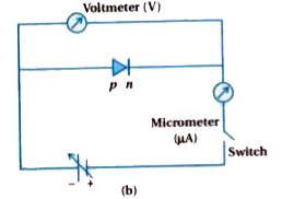
The circuit arrangement for reverse characteristics of the p-n junction diode is shown in the figure (b).

The battery is connected to the diode through a potentiometer or reheostat so that the applied voltage to the diode can be changed.
For different values of voltages, the value of the current is noted. A graph between V and I is obtained as in figure (c ) question 30. Here current is of the order of .
The current under reverse bias is essentially voltage independent upto a critical reverse bias voltage known as breakdown voltage .
When reverse bias voltage becomes equal to break down voltage , the diode reverse current increases sharply. Even or slight increase in the bias voltage causes large change in the current.
If the reverse current is not limited by an external circuit below the rated value, the p-n junction will get destroyed. Once it exceeds the rated value, the diode gets destroyed due to overheating.
For the diode in reverse bias, the current is very small with opposite direction and almost remains constant with change in bias. It is called reverse saturation current.
The general purpose diode are not used beyond the reverse saturation current region.
For diode, a quantity called dynamic resistance as the ratio of small change in voltage to a small change in current
The resistance of the diode in forward bias mode is approximately between to in reverse bias mode it is about of the order .
Topper's Solved these Questions
- SEMICONDUCTOR ELECTRONICS : MATERIALS, DEVICES AND SIMPLE CIRCUITS Book:KUMAR PRAKASHANChapter:SEMICONDUCTOR ELECTRONICS : MATERIALS, DEVICES AND SIMPLE CIRCUITS Exercise:Section-B : Numericals (Numerical From Textual illustrations)
Explore 16 Videos
- SEMICONDUCTOR ELECTRONICS : MATERIALS, DEVICES AND SIMPLE CIRCUITS Book:KUMAR PRAKASHANChapter:SEMICONDUCTOR ELECTRONICS : MATERIALS, DEVICES AND SIMPLE CIRCUITS Exercise:Section-B : Numericals (Numerical From Textual Exercise)
Explore 15 Videos
- SEMICONDUCTOR ELECTRONICS : MATERIALS, DEVICES AND SIMPLE CIRCUITS Book:KUMAR PRAKASHANChapter:SEMICONDUCTOR ELECTRONICS : MATERIALS, DEVICES AND SIMPLE CIRCUITS Exercise:Section-D : Multiple Choice Questions (MCQs) (MCQs asked in Competitive Exams)
Explore 129 Videos
- SAMPLE QUESTION PAPER Book:KUMAR PRAKASHANChapter:SAMPLE QUESTION PAPER Exercise:PART-B SECTION-C
Explore 5 Videos
- WAVE OPTICSBook:KUMAR PRAKASHANChapter:WAVE OPTICSExercise:SECTION-D (MULTIPLCE CHOICE QUESTIONS (MCQS)) (MCQS FROM DARPAN BASED ON TEXTBOOK)
Explore 239 Videos
Similar Questions
C, Si and Ge have same lattice structure. Why is C insulator while Si and Ge intrinsic semiconductors?
View SolutionIn an n type silicon, which of the following statements is true:
View SolutionAt absolute zero temperature Si acts as ……..
View SolutionTwo charges –q and +q are located at points (0, 0, –a) and (0, 0, a), respectively.
(a) What is the electrostatic potential at the points (0, 0, z) and (x, y, 0) ?
(b) Obtain the dependence of potential on the distance r of a point from the origin when r/a>>1 .
(c) How much work is done in moving a small test charge from the point (5,0,0) to (–7,0,0) along the x-axis? Does the answer change if the path of the test charge between the same points is not along the x-axis?
View SolutionAccording to particle theory of light what is the velocity of light in a dense medium, compared to that in rare medium ?
View SolutionExplain briefly with the help of necessary diagram, the forward and the reverse biasing of p-n junction diode. Also draw their characteristic curves in the two cases.
View SolutionExplain (i) forward biasing (ii) reverse biasing of a P-N junction diode. With the help of a circuit diagram, explain the use of this device as a half wave rectifier.
View SolutionWhat is a p-n junction diode? Define the term 'dynamic resistance' for the junction diode. With the help of a circuit diagram explain the working of a p-n junction diode as a full wave rectifier.
View SolutionExplain the working of p-n junction diode in forward and reverse biased mode.
View Solutionp -n संधि डायोड की उत्क्रम अभिनत क्रिया परिपथ चित्र की सहायता से समझाइए। इसका उपयोग जेनर डायोड में कैसे होता है?
View SolutionDraw the circuit diagram of a forward biased and reverse biased p-n junction diode.
View SolutionExplain the working of a reverse biased p-n junction diode.
View SolutionDraw the circuit arrangement for studying the V - I characteristics of a p-n junction diode in (i) forward and (ii) reverse bias. Briefly explain how the typical V - I characteristics of a diode are obtained and draw these characteristics.
View SolutionExplain the forward characteristics of the p-n junction diode by drawing circuit and graph.
View SolutionExplain briefly with the help of necessary diagram, the forward and the reverse biasing of p-n junction diode. Also draw their characteristic curves in the two cases.
View Solution

