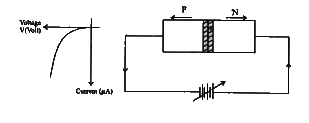
Explain the working of a reverse biased p-n junction diode.Solution in Kannada
Reverse Bias: When battery is connected across the junction such that p side is connected to the negative terminal and n side to the positive terminal, the p-n junction is said to be reverse baised. In this case the applied voltage adds to the effect of junction p.d and hence majority carriers cannot cross the junction. the current through the circuit is practically zero.
thus reverse bias offers a very high resistance but small current of the order of a few mA flows through the circuit due to the minority carriers in the p and n regions. As the applied voltage is gradually increased a very large current results at a particular this voltage is called the break down or cut-in voltage.

Topper's Solved these Questions
- SEMICONDUCTOR ELECTRONICSBook:SUBHASH PUBLICATIONChapter:SEMICONDUCTOR ELECTRONICSExercise:FIVE MARKS QUESTIONS WITH ANSWERS
Explore 9 Videos
- SEMICONDUCTOR ELECTRONICSBook:SUBHASH PUBLICATIONChapter:SEMICONDUCTOR ELECTRONICSExercise:OPTIONAL NUMERICALS WITH SOLUTIONS
Explore 6 Videos
- SEMICONDUCTOR ELECTRONICSBook:SUBHASH PUBLICATIONChapter:SEMICONDUCTOR ELECTRONICSExercise:OPTIONAL NUMERICALS WITH SOLUTIONS
Explore 6 Videos
- RAY OPTICS AND OPTICAL INSTRUMENTSBook:SUBHASH PUBLICATIONChapter:RAY OPTICS AND OPTICAL INSTRUMENTSExercise:NUMERICALS WITH SOLUTIONS
Explore 22 Videos
- SUPER MODEL QUESTION PAPER ( WITH ANSWERS ) Book:SUBHASH PUBLICATIONChapter:SUPER MODEL QUESTION PAPER ( WITH ANSWERS ) Exercise:PART D
Explore 26 Videos
Similar Questions
What is half wave rectification? Explain the working of a half wave rectifier. Indicate the waveforms of input and output voltage.
View SolutionIf the peak value voltage in the secondary output ac voltage is 12V, then what will be the average DC in the case of HWR and FWR?
View SolutionIf the peak value voltage in the secondary output ac voltage is 12V, then what will be the average DC in the case of HWR and FWR?
View SolutionShow that lateral shift is equal to the thickness of the slab for grazing incidence.
View SolutionDerive an expression for electrical conductivity.
View SolutionWhen the p−n junction diode is reverse biased, the thickness of the depletion layer
View SolutionA p-n junction diode is reverse biased. Then
View SolutionExplain the working of a pn-junction diode in forward- and reverse-biased modes.
View SolutionExplain the working of p-n junction diode in forward and reverse biased mode.
View SolutionWhen a p-n junction diode is reverse biased
View SolutionExplain the working of a forward biased p-n junction diode.
View SolutionIf a p-n junction diode is reverse biased, then the resistance measured by an ohm-meter will be
View SolutionIf a p-n junction diode is reverse biased, then the resistance measured by an ohm-meter will be
View SolutionThe reverse biasing in a p-n junction diode
View SolutionWhich of the following shows a reverse biased p-n junction diode ?
View Solution

