Explain the change in the band with the temperature of the intrinsic semiconductor by drawing figure. Solution in Gujrati
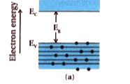
An intrinsic semiconductor will behave like an insulator at T = 0K as shown in figure (a).

At T = 0K temperature all the electrons are bound in the valence band and they are not in conduction band so electrons cannot flow, as a result it behave as insulators.
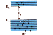
These thermally exicted electrons at T>0K, partially occupy the conduction band which is shown in figure.

Solid dots indicates electrons while empty dot indicates holes in the figure.
As shown in the figure, four electrons getting energy from valence band and have gone into conduction band so four holes shown in valence band.
Topper's Solved these Questions
- BOOK - KUMAR PRAKASHANCHAPTER - SEMICONDUCTOR ELECTRONICS : MATERIALS, DEVICES AND SIMPLE CIRCUITS EXERCISE - Section-B : Numericals (Numerical From Textual illustrations)16videos
SEMICONDUCTOR ELECTRONICS : MATERIALS, DEVICES AND SIMPLE CIRCUITS
- BOOK - KUMAR PRAKASHANCHAPTER - SEMICONDUCTOR ELECTRONICS : MATERIALS, DEVICES AND SIMPLE CIRCUITS EXERCISE - Section-B : Numericals (Numerical From Textual Exercise)15videos
SEMICONDUCTOR ELECTRONICS : MATERIALS, DEVICES AND SIMPLE CIRCUITS
- BOOK - KUMAR PRAKASHANCHAPTER - SEMICONDUCTOR ELECTRONICS : MATERIALS, DEVICES AND SIMPLE CIRCUITS EXERCISE - Section-D : Multiple Choice Questions (MCQs) (MCQs asked in Competitive Exams)129videos
SEMICONDUCTOR ELECTRONICS : MATERIALS, DEVICES AND SIMPLE CIRCUITS
- BOOK - KUMAR PRAKASHANCHAPTER - SAMPLE QUESTION PAPER EXERCISE - PART-B SECTION-C5videos
SAMPLE QUESTION PAPER
- BOOK - KUMAR PRAKASHANCHAPTER - WAVE OPTICSEXERCISE - SECTION-D (MULTIPLCE CHOICE QUESTIONS (MCQS)) (MCQS FROM DARPAN BASED ON TEXTBOOK)239videos
WAVE OPTICS
Similar Questions
C, Si and Ge have same lattice structure. Why is C insulator while Si and Ge intrinsic semiconductors?
02:35View SolutionIn an n type silicon, which of the following statements is true:
02:13View SolutionAt absolute zero temperature Si acts as ……..
04:26View SolutionTwo charges –q and +q are located at points (0, 0, –a) and (0, 0, a), respectively.
(a) What is the electrostatic potential at the points (0, 0, z) and (x, y, 0) ?
(b) Obtain the dependence of potential on the distance r of a point from the origin when r/a>>1 .
(c) How much work is done in moving a small test charge from the point (5,0,0) to (–7,0,0) along the x-axis? Does the answer change if the path of the test charge between the same points is not along the x-axis?02:24View SolutionAccording to particle theory of light what is the velocity of light in a dense medium, compared to that in rare medium ?
04:35View SolutionHow does the conductivity and resistivity change with rise of temperature in case of intrinsic semiconductor?
12:42View SolutionThe fraction (f) of the number of electrons raised from valence band to conduction band at temperature TK in intrinsic semiconductor is given by........
02:50View SolutionExpalin the formation of energy band in solids. Draw energy band diagram for (i) and conductor (ii) and intrinsic semiconductor.
03:50View SolutionThe probability of electrons to be found in the conduction band of an intrinsic semiconductor at a finite temperature
04:25View SolutionDraw the energy band diagram of an intrinsic semiconductor.
02:45View SolutionExplain how an intrinsic semiconductor can be converted into an n-type semiconductor and a p-type semiconductors. Draw the energy band diagrams of n-type and p-type semicon ductors.
48:30View Solutionp- प्रकार के अर्धचालक का ऊर्जा बैंड आरेख खीचिए | ताप बढ़ाने पर नेज अर्धचालक का वर्टीज ऊर्जा अंतराल की प्रकार परिवर्तित होता है ?
02:34View SolutionDraw energy band diagram of an intrinsic semiconductor at room temperature.
View SolutionExplain the difference between intrinsic semiconductors and extrinsic semiconductors.
03:17View SolutionThe probability of electrons to be found in the conduction band of an intrinsic semiconductor at a finite temperature
02:30View Solution
