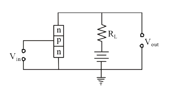
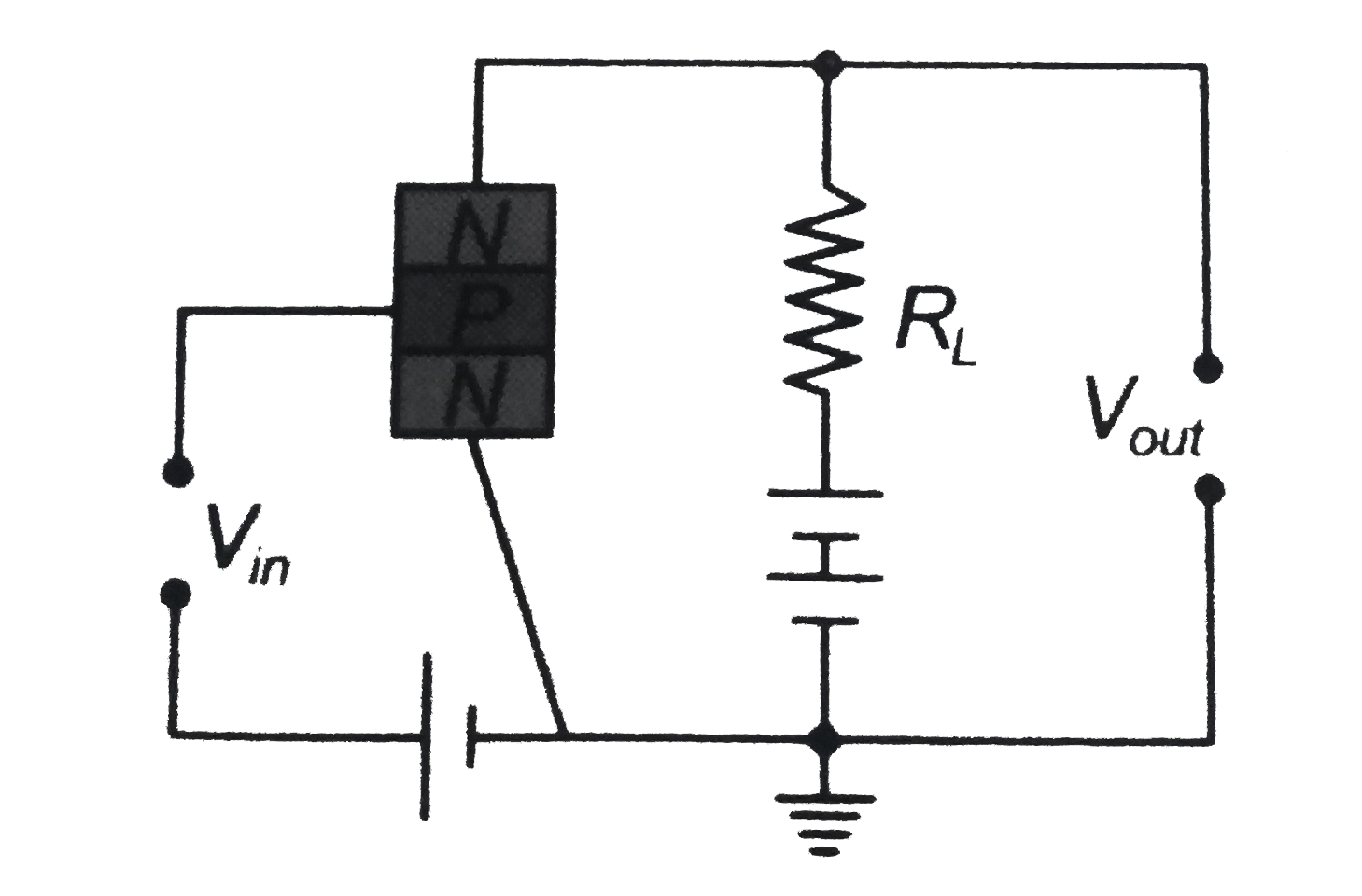
An NPN-transistor circuit is arranged as shown in figure. It is
A
A common base amplifier circuit
B
A common emitter amplifier circuit
C
A common collector amplifier circuit
D
Neither of the above
Video Solution
Text Solution
The correct Answer is:B
Because emitter (N) is common to both, base (P) and collector (N).
|
Topper's Solved these Questions
- SEMICONDUCTOR ELECTRONICSBook:A2ZChapter:SEMICONDUCTOR ELECTRONICSExercise:Digital Electronics
Explore 40 Videos
- SEMICONDUCTOR ELECTRONICSBook:A2ZChapter:SEMICONDUCTOR ELECTRONICSExercise:Problems Based On Mixed Concepts
Explore 32 Videos
- SEMICONDUCTOR ELECTRONICSBook:A2ZChapter:SEMICONDUCTOR ELECTRONICSExercise:Diode In Circuits
Explore 40 Videos
- NUCLEAR PHYSICSBook:A2ZChapter:NUCLEAR PHYSICSExercise:Section D - Chapter End Test
Explore 29 Videos
- SOURCE AND EFFECT OF MAGNETIC FIELDBook:A2ZChapter:SOURCE AND EFFECT OF MAGNETIC FIELDExercise:Section D - Chapter End Test
Explore 30 Videos
Similar Questions
Knowledge Check
The arrangement as shown in figure is called as
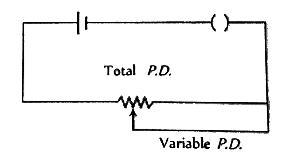 APotential dividerBPotential adderCPotential substracterDPotential multiplier
A circuit is arranged as shown. Then, the current from A to B is
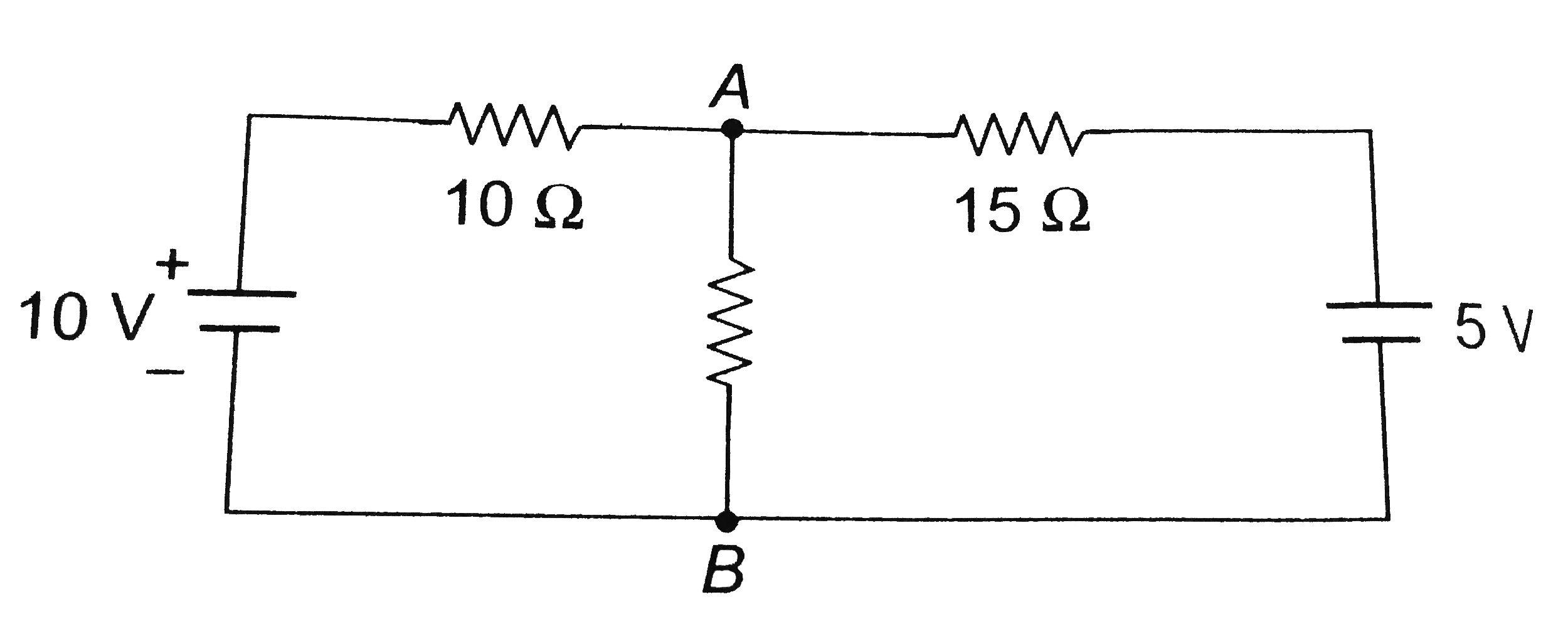 A+500mAB+1.5mAC−250mAD−500mA
In the circuit as shown in figure the
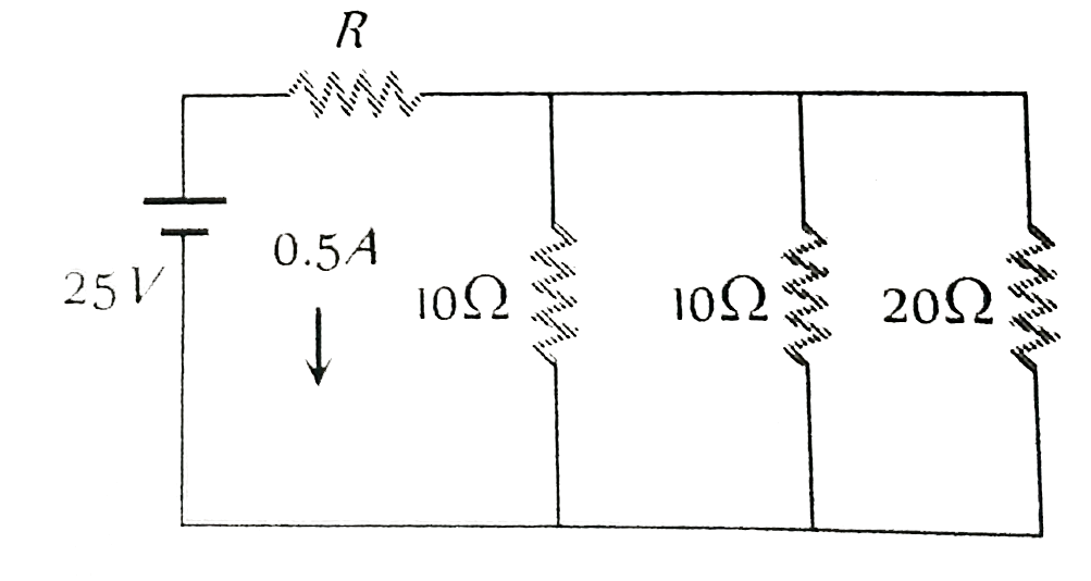 AResistance R=46ΩBCurrent through 20Ω resistance is 0.1ACPotential difference across the middle resistance is 2VDAll option are correct
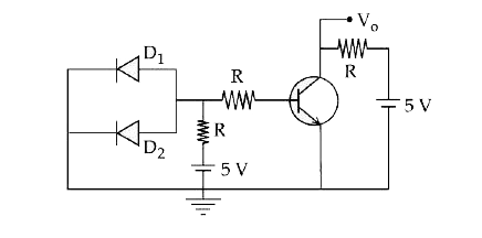
A circuit is arranged as shown in figure. The output voltage V0 is equal to ____________V.
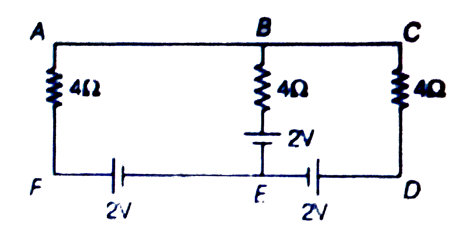
View SolutionIn the circuit shown in figure
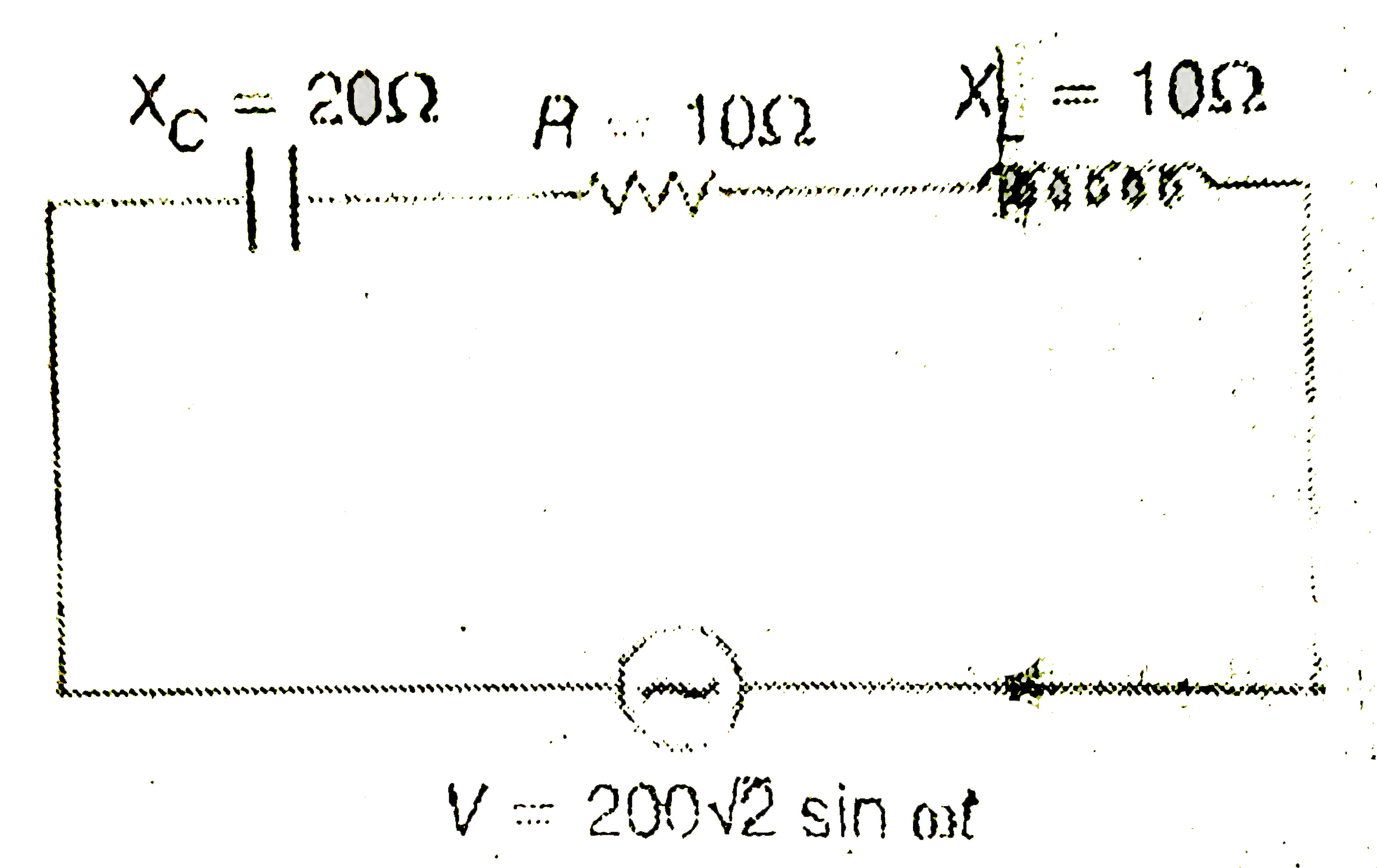
View SolutionIn LCR circuit as shown in figure
View SolutionThe circuit as shown in figure is equivalent to

View SolutionThe circuit as shown in figure is equivalent to

View Solution


