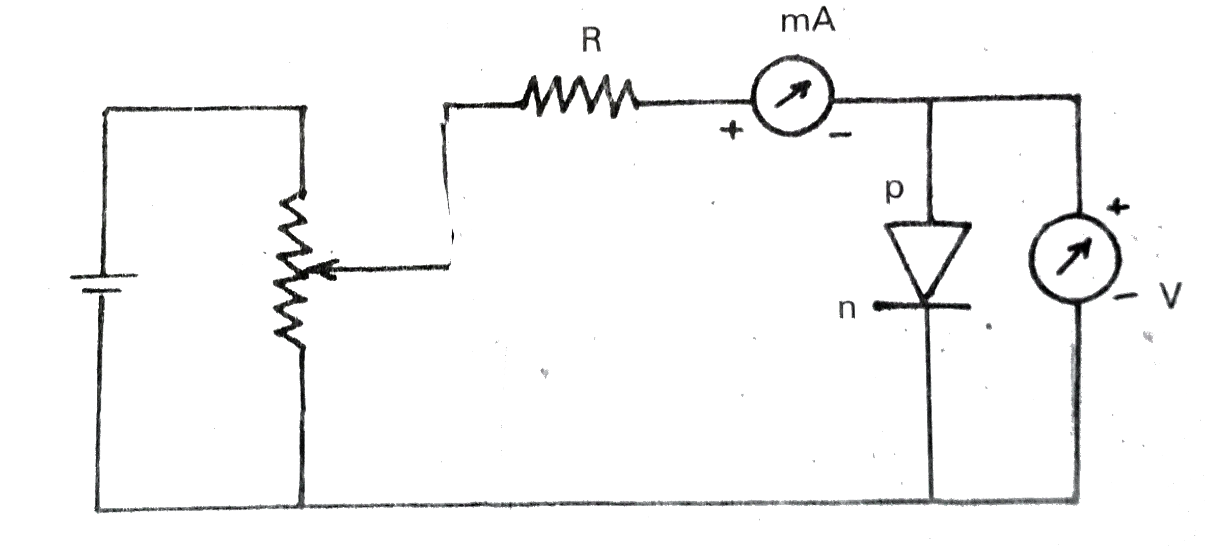
Draw and explain the current -voltage (I-V) characteristic curves of a junction diode in forward and reverse bias. Solution in Telugu
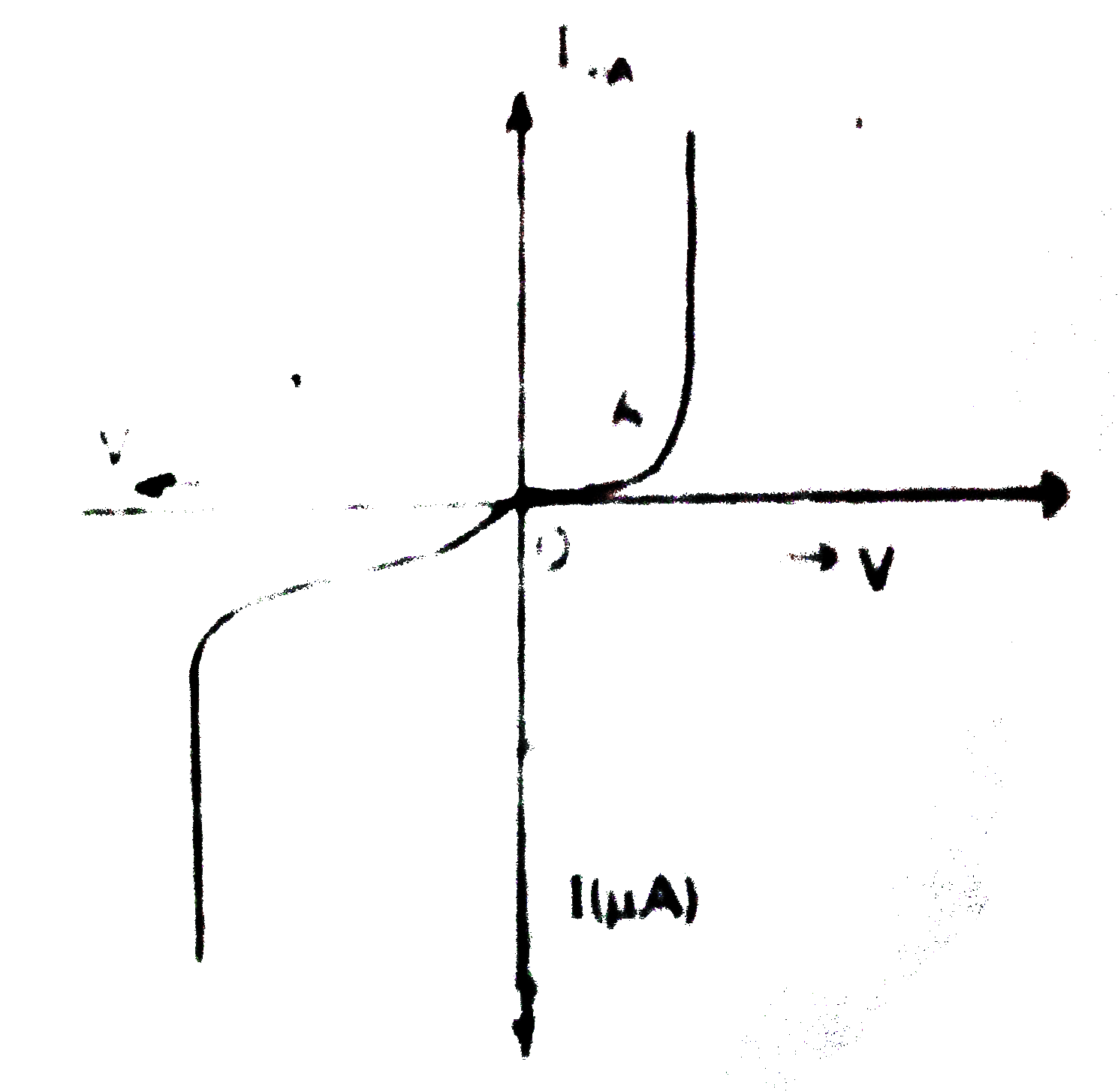
A graph is drawn between the applied voltage ( V) and the current (I) passing through the p-n junction diode is called characteristics of a diode.

As forward bias voltage is increased potential barrier decreases, but initially increases in current is negligible ( region OA) . This is due to the potential barrier .
The voltage at which the current starts to increase rapidely is calle knee voltage ( or ) cut in voltage.
In this reverse bias, small current flows in the circuit due to minority charge carriers. If the reverse voltage is increased further, after some voltage , there will be a sudden rise of reverse current. This region is named as breakdown region.

Topper's Solved these Questions
- SEMICONDUCTOR ELECTRONICS : MATERIALS , DEVICES , AND SIMPLE CIRCUITS Book:VIKRAM PUBLICATION ( ANDHRA PUBLICATION)Chapter:SEMICONDUCTOR ELECTRONICS : MATERIALS , DEVICES , AND SIMPLE CIRCUITS Exercise:LONG ANSWER QUESTIONS
Explore 7 Videos
- SEMICONDUCTOR ELECTRONICS : MATERIALS , DEVICES , AND SIMPLE CIRCUITS Book:VIKRAM PUBLICATION ( ANDHRA PUBLICATION)Chapter:SEMICONDUCTOR ELECTRONICS : MATERIALS , DEVICES , AND SIMPLE CIRCUITS Exercise:TEXTUAL EXERCISES
Explore 11 Videos
- SEMICONDUCTOR ELECTRONICS : MATERIALS , DEVICES , AND SIMPLE CIRCUITS Book:VIKRAM PUBLICATION ( ANDHRA PUBLICATION)Chapter:SEMICONDUCTOR ELECTRONICS : MATERIALS , DEVICES , AND SIMPLE CIRCUITS Exercise:VERY SHORT ANSWER QUESTIONS
Explore 14 Videos
- RAY OPTICAL AND INSTRUMENTSBook:VIKRAM PUBLICATION ( ANDHRA PUBLICATION)Chapter:RAY OPTICAL AND INSTRUMENTSExercise:TEXTUAL EXERCISES
Explore 60 Videos
- TELANGANA MARCH-2019Book:VIKRAM PUBLICATION ( ANDHRA PUBLICATION)Chapter:TELANGANA MARCH-2019Exercise:SECTION -B
Explore 5 Videos
Similar Questions
What is a junction diode ? Explain the formation of depletion region at the junction. Explain the variation of depletion region in forward and reverse-biased condition.
View SolutionIn an n-type silicon, which of the following statement is true :
(a) Electrons are majority carriers are trivalent atoms are the dopants.
(b) Electrons are minority carriers and pentavalent atoms are the dopants.
(c ) Holes are minority carriers and pentavalent atoms are the dopants.
(d ) Holes are majority carriers and trivalent atoms are the dopants.
View SolutionWhat is an n-type semiconductor ? What are the majority and minority charge carriers in it?
View SolutionA small candal, 2.5 cm in size is placed at 27 cm in front of a concave mirror of radius of curvature 36 cm. At wht distance from the mirror should a screen be placed in order to obtain a sharp image ? Describe the nature and size of the image. If the candale is moved closer to the mirror, how would the screen have to be moved ?
View SolutionExplain the formation of Mirage .
View SolutionIn V-I characteristics of a p-n junction diode, why is the current under reverse bias almost independence of the applied potential upto a critical voltage?
View SolutionExplain the working of a semiconductor diode when it is forward biased. Draw the I-V characteristics for both forward bias and reverse bias of a semiconductor diode.
View SolutionDraw the V-I characterisitics of p-n junction diode in forward bias and in reverse bias.
View SolutionDraw the graph showing the variation of current with voltage for a p-n junction diode in forward bias as well as revese bias arrangements.
View SolutionExplain briefly, with the help of circuit diagram , how V-I characteristics of a p-n junction diode are obtained in (i) forward bias, and (ii) reverse bias. Draw the shapes of the characteristic curves obtained. Or Explain briefly, with the help of necessary diagrams, the forward and the reverse biasing of a p-n junction diode. Also draw their characteristic curves in the two cases.
View SolutionExplain the working of a forward biased p-n junction diode.
View SolutionDraw the circuit arrangement for studying the V - I characteristics of a p-n junction diode in (i) forward and (ii) reverse bias. Briefly explain how the typical V - I characteristics of a diode are obtained and draw these characteristics.
View SolutionIn V-I characteristics of a p-n junction diode, why is the current under reverse bias almost independent of the applied potential upto a critical voltage?
View SolutionExplain forward bias and reverse bias of the junction diode.
View SolutionWhat is junction diode ? How is depletion layer formed ? Draw its forward and reverse bias characteristics by showing biasing of diodes ?
View Solution

