What is a junction diode ? Explain the formation of depletion region at the junction. Explain the variation of depletion region in forward and reverse-biased condition. Solution in Telugu
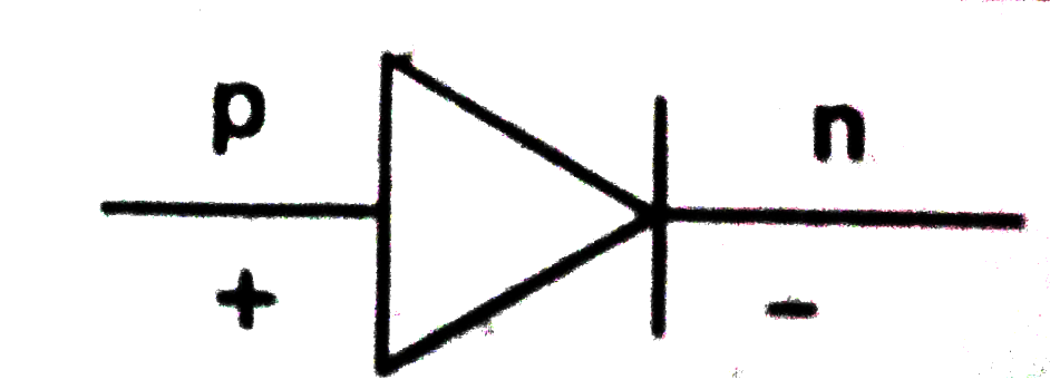
p-n junction diode When a p-type semiconductor is suitably joined to n-type semiconductor, a p-n junction diode is formed.
The circuit symbol of p-n junction diode is shown in figure.
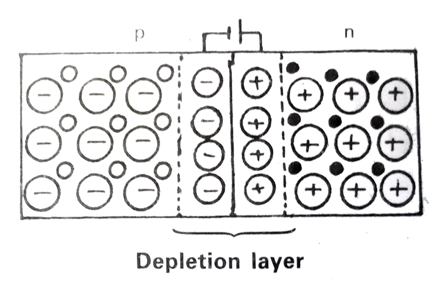
Formation of depletion layer at the junction When p-n junction is formed, the free electrons on n-side diffuse over to p-side , they combine with holes and become neutral. Similarly holeson p-side diffuse over to n-side and combine with electrons become neutral.

This results in a narrow region formed on either side of the junction. This region is called depletion layer. Depletion layer is free from charge carriers.
The n-type material near the junction becomes positively charged due to immobile donor ions andp-type material becomes negatively charged due to immobile acceptor ions. This creates an electric field near the junction directed from n-region to p-region and cause a potential barrier.
The potential barrier stops further diffusion of holes and electrons across the junction.The value of the potential barrier depends upon the nature of the crystal, its temperature and the amount of doping.

Forward bias
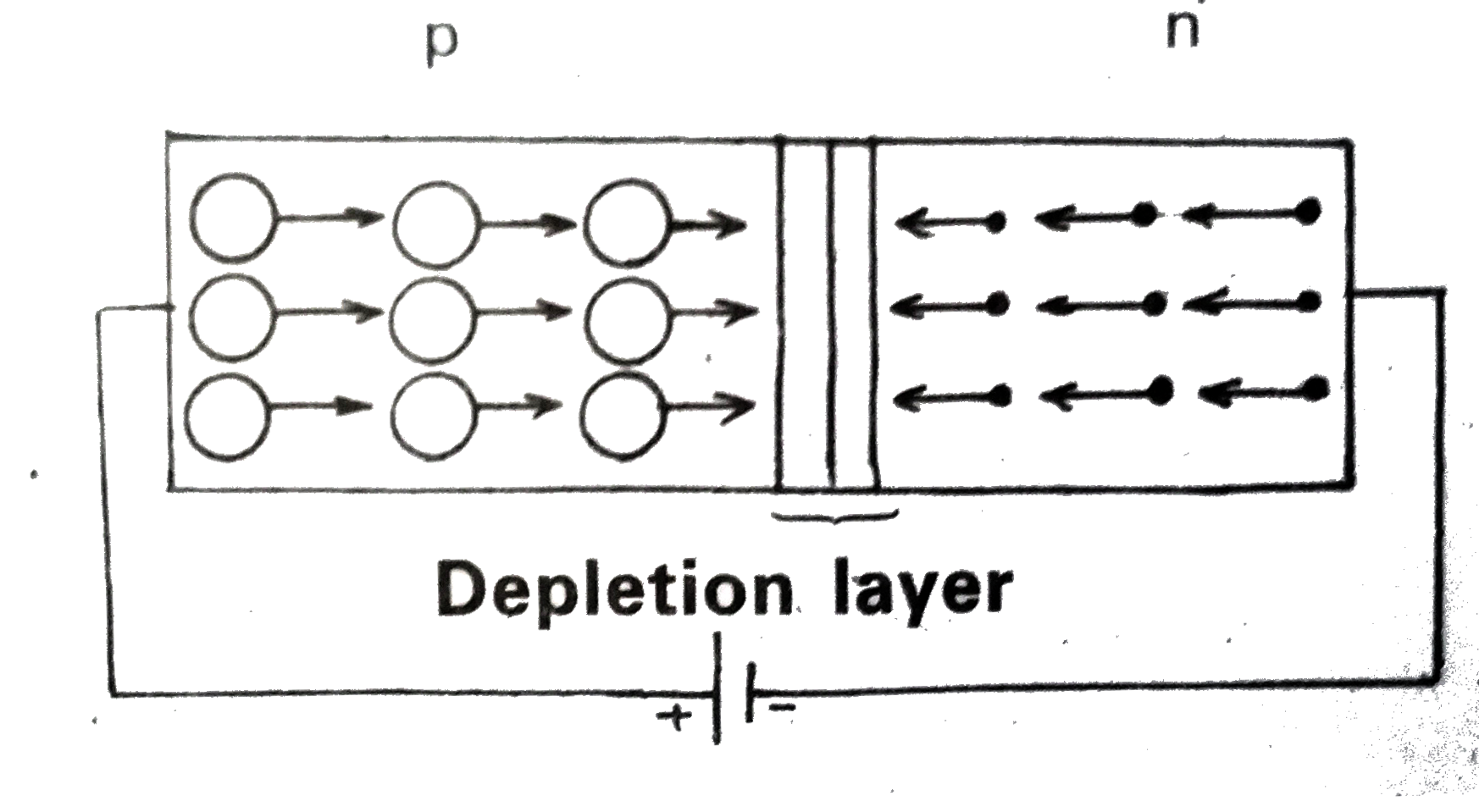
"When a positive terminal of a battery is connected to p-side and negative terminal is connected to n-side, then p-n junction diode is said to be forward bias ".
The holesin the p-region are repelled by the positive polarity and
 move towards the junction. Similarly electron in the n-region are repelled by the negative polarity and move towards the junction.
As a result, the width of the depletion layer decreases.The charge carriers cross the junction and electric current flows in the circuit.
Hence in forward bias resistance of diode is low. This position is called switch on position.
Reverse bias

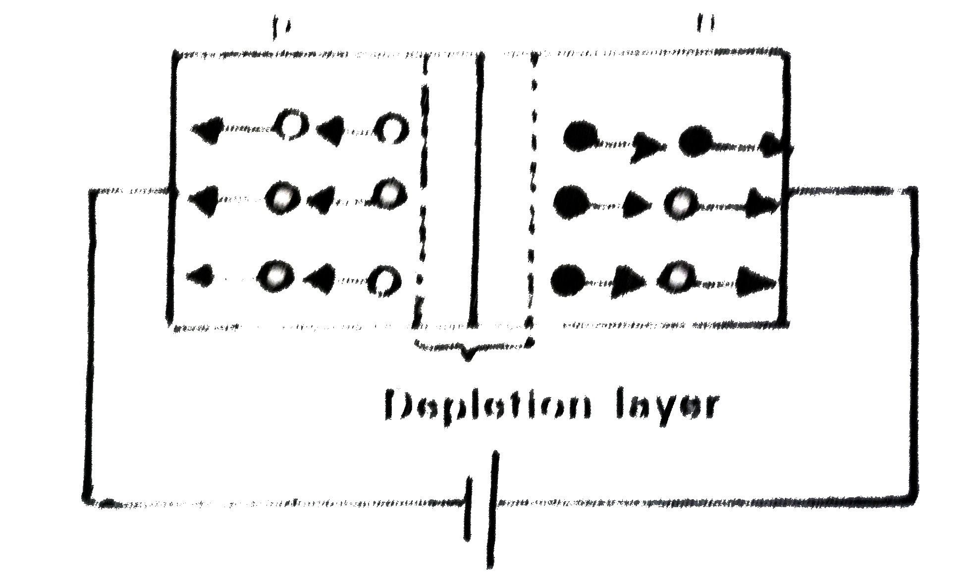
"When the negative terminal of the battery is connected to p-side and positive terminal of the battery is connected n-side of the p-n junction, then the diode is said to be reverse bias".
The holes in the p-region are attracted towards negative polarity and move away from the junction . Similarly the electron in the n-region are attracted towards positive polarity and move away, from the junction.
So, which of the depletion layer and potential barrier increases. Hence resistance of p-n junction diode increases. Thus the reverse biased diode is called switch off position.
Topper's Solved these Questions
- SEMICONDUCTOR ELECTRONICS : MATERIALS , DEVICES , AND SIMPLE CIRCUITS Book:VIKRAM PUBLICATION ( ANDHRA PUBLICATION)Chapter:SEMICONDUCTOR ELECTRONICS : MATERIALS , DEVICES , AND SIMPLE CIRCUITS Exercise:TEXTUAL EXERCISES
Explore 11 Videos
- SEMICONDUCTOR ELECTRONICS : MATERIALS , DEVICES , AND SIMPLE CIRCUITS Book:VIKRAM PUBLICATION ( ANDHRA PUBLICATION)Chapter:SEMICONDUCTOR ELECTRONICS : MATERIALS , DEVICES , AND SIMPLE CIRCUITS Exercise:ADDITIONAL EXERCISES
Explore 8 Videos
- SEMICONDUCTOR ELECTRONICS : MATERIALS , DEVICES , AND SIMPLE CIRCUITS Book:VIKRAM PUBLICATION ( ANDHRA PUBLICATION)Chapter:SEMICONDUCTOR ELECTRONICS : MATERIALS , DEVICES , AND SIMPLE CIRCUITS Exercise:SHORT ANSWER QUESTIONS
Explore 16 Videos
- RAY OPTICAL AND INSTRUMENTSBook:VIKRAM PUBLICATION ( ANDHRA PUBLICATION)Chapter:RAY OPTICAL AND INSTRUMENTSExercise:TEXTUAL EXERCISES
Explore 60 Videos
- TELANGANA MARCH-2019Book:VIKRAM PUBLICATION ( ANDHRA PUBLICATION)Chapter:TELANGANA MARCH-2019Exercise:SECTION -B
Explore 5 Videos
Similar Questions
In an n-type silicon, which of the following statement is true :
(a) Electrons are majority carriers are trivalent atoms are the dopants.
(b) Electrons are minority carriers and pentavalent atoms are the dopants.
(c ) Holes are minority carriers and pentavalent atoms are the dopants.
(d ) Holes are majority carriers and trivalent atoms are the dopants.
View SolutionThe Number of silicon atoms per m3 is 5×1028 . This is doped simultaneously with 5×10²² atoms per m3 of Arsenic and 5×10²⁰ per m^(3) atoms of Indium. Calculate the number of electron and holes. Given that ni=1.5×10¹⁶m−3. Is the material n-type or p-type ?
View SolutionWhat are n-type and p-type semiconducts ?How is a semiconductor junction formed ?
View SolutionA small candal, 2.5 cm in size is placed at 27 cm in front of a concave mirror of radius of curvature 36 cm. At wht distance from the mirror should a screen be placed in order to obtain a sharp image ? Describe the nature and size of the image. If the candale is moved closer to the mirror, how would the screen have to be moved ?
View SolutionExplain the formation of Mirage .
View SolutionIn a forward biased PN- junction diode, the potential barrier in the depletion region is of the from...
View SolutionWhat is meant by depletion region in a junction diode? How is this region formed?
View SolutionIn a forward biased p-n junction diode, the potential barrier in the depletion region will be of the form
View SolutionExplain what happens to the depletion layer ,if the junction is forward biased and reverse biased.
View SolutionWhat will be the change in the thickness of depletion region if a p-n junction is forward biased ?
View SolutionWhat is depletion region in p-n junction diode. Explain its formation with the help of a suitable diagram.
View SolutionIn the depletion region of the an unbaised p-n junction diode, there are
View SolutionWhat is meant by depletion region in a junction diode? How is this region formed?
View SolutionWhat is junction diode ? How is depletion layer formed ? Draw its forward and reverse bias characteristics by showing biasing of diodes ?
View SolutionWhat happens to the width of the depletion layer in ap.n junction diode when it is
1) forward-biased and
2) reverse -biased ?
View Solution

