Describe a transistor and explain its working. Solution in Telugu
Transistor : It is a device which consists of two p-n junctions joined back to back.Transistor means transfer of resistance.
(i)Emitter (E ) : The section at one end of transistor is called emitter. It is heavily doped region.It emitts charge carriers.
(2) Base ( B) : The middle section of transistor is called base. This is lightly doped and very thin and almost of the charge carriers injected into it toflow into collector with out neutralised.
(3) Collector (C ) : The section at the other end is called collector.It is moderately doped. It collects the charge carrers. Physically it is large.
.Note : Usually the emitter-base junction is forward biased and collector-base junction is revrse biased.
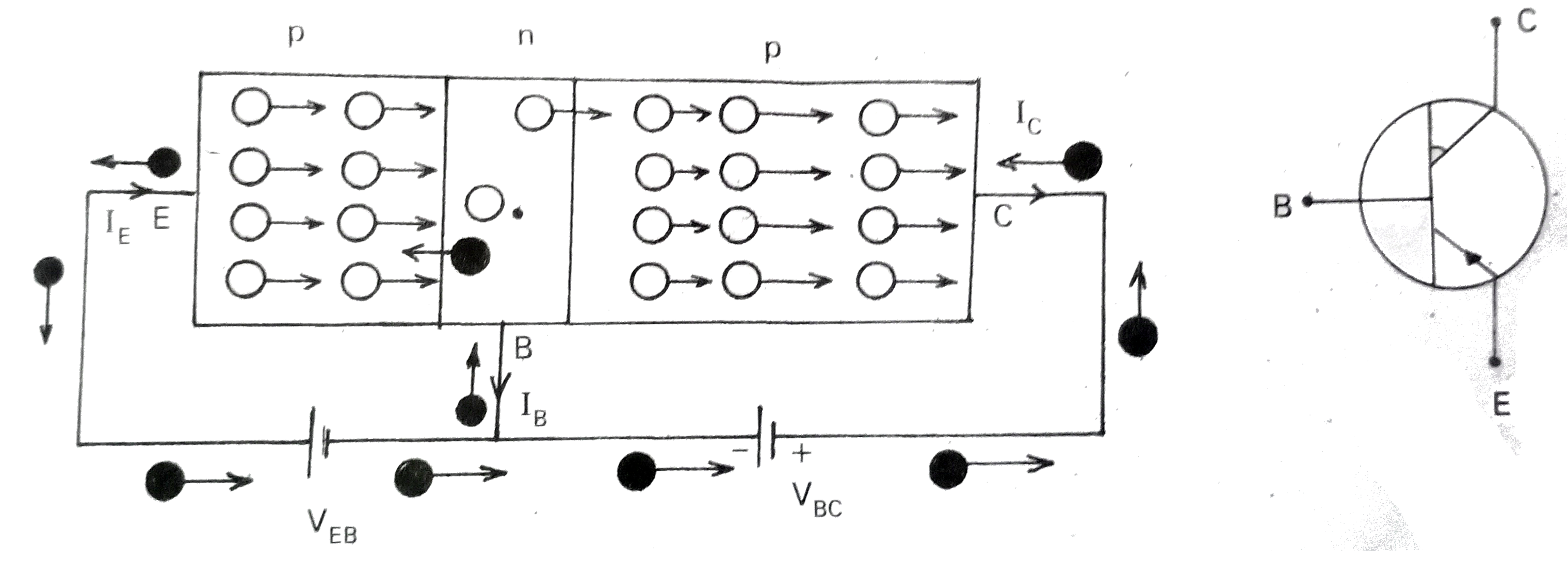
Working of p-n transistor : The base part is made of n-type, emitter and collector parts are made ofp-type . The circuit symbol of p-n-p transistor is shown in figure.

The emitter junction is forward biased by connecting positive terminal of battery to the emitter and negative to the base. The collector junction is reverse biased by connecting negative to the collector and positive to the base.
The holesin p-region(emitter) are repelledby the positive terminal and crossing ther emitter junction,enterthe base region causing emitter current IE.Few holes are combined with electrons in base region, this constitue base current (IB).Majority of holes enters through the collector region. The negative terminal battery rapidly sweeps the holes in the collector region causing collector current (IC).
IE=IB+IC
IN p-n-p transistor inside the circuit charge carriers are holes and outside the circuit charge carriers are electrons.
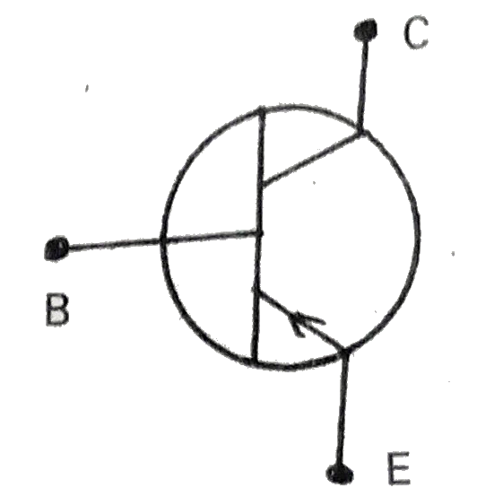
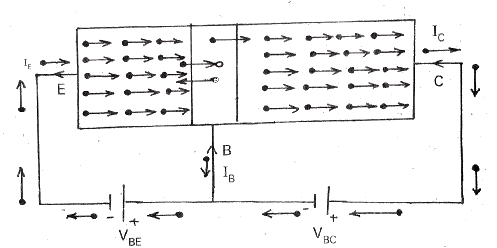
n-p-n transistor : If the basepart is made of p-type, emitter and collector parts aremade of n-type,we get n-p-n transistor. The circuit symbol of n-p-n transistor is shown in figure.


The emitter junction is forward biased with negative end of a battery connectedto emitter and positive to the base. The collector junction is reverse biased with collector positive end of a battery and negative to the base.
The electrons in the emitter ( n - region) are repelled by the negative terminal of a battery and cross the base region constituting the emitter current IE. A small number of electrons may recombine with holes in base region constituting base current IB.
Majority charge carriers ( electrons ) enter into the collector region. The positive terminal of a battery rapidly sweeps the electrons in collector, constituting collector current IC.
IE=IB+IC
In n-p-n transistor charge carriers inside and outside the circuit are electrons.
Topper's Solved these Questions
- SEMICONDUCTOR ELECTRONICS : MATERIALS , DEVICES , AND SIMPLE CIRCUITS BOOK - VIKRAM PUBLICATION ( ANDHRA PUBLICATION)CHAPTER - SEMICONDUCTOR ELECTRONICS : MATERIALS , DEVICES , AND SIMPLE CIRCUITS EXERCISE - TEXTUAL EXERCISES
11 Videos
- SEMICONDUCTOR ELECTRONICS : MATERIALS , DEVICES , AND SIMPLE CIRCUITS BOOK - VIKRAM PUBLICATION ( ANDHRA PUBLICATION)CHAPTER - SEMICONDUCTOR ELECTRONICS : MATERIALS , DEVICES , AND SIMPLE CIRCUITS EXERCISE - ADDITIONAL EXERCISES
8 Videos
- SEMICONDUCTOR ELECTRONICS : MATERIALS , DEVICES , AND SIMPLE CIRCUITS BOOK - VIKRAM PUBLICATION ( ANDHRA PUBLICATION)CHAPTER - SEMICONDUCTOR ELECTRONICS : MATERIALS , DEVICES , AND SIMPLE CIRCUITS EXERCISE - SHORT ANSWER QUESTIONS
16 Videos
- RAY OPTICAL AND INSTRUMENTSBOOK - VIKRAM PUBLICATION ( ANDHRA PUBLICATION)CHAPTER - RAY OPTICAL AND INSTRUMENTSEXERCISE - TEXTUAL EXERCISES
60 Videos
- TELANGANA MARCH-2019BOOK - VIKRAM PUBLICATION ( ANDHRA PUBLICATION)CHAPTER - TELANGANA MARCH-2019EXERCISE - SECTION -B
5 Videos
Similar Questions
In an n-type silicon, which of the following statement is true :
(a) Electrons are majority carriers are trivalent atoms are the dopants.
(b) Electrons are minority carriers and pentavalent atoms are the dopants.
(c ) Holes are minority carriers and pentavalent atoms are the dopants.
(d ) Holes are majority carriers and trivalent atoms are the dopants.
View SolutionThe Number of silicon atoms per m3 is 5×1028 . This is doped simultaneously with 5×10²² atoms per m3 of Arsenic and 5×10²⁰ per m^(3) atoms of Indium. Calculate the number of electron and holes. Given that ni=1.5×10¹⁶m−3. Is the material n-type or p-type ?
View SolutionWhat are n-type and p-type semiconducts ?How is a semiconductor junction formed ?
View SolutionA small candal, 2.5 cm in size is placed at 27 cm in front of a concave mirror of radius of curvature 36 cm. At wht distance from the mirror should a screen be placed in order to obtain a sharp image ? Describe the nature and size of the image. If the candale is moved closer to the mirror, how would the screen have to be moved ?
View SolutionExplain the formation of Mirage .
View SolutionDescribe a pith ball electroscope and explain its working.
View Solutionp - n - p ट्रांजिस्टर की संरचना का वर्णन कीजिए तथा परिपथ चित्र देते हुए समझाइए की यह उभयनिष्ठ-उत्सर्जक विन्यास में वोल्टता प्रवर्धक का कार्य कैसे करता है ?
View Solutionn - p - n ट्रांजिस्टर की रचना एवं कार्यविधि का वर्णन कीजिए तथा प्रवर्धक के रूप में इसके कार्यों की संक्षिप्त व्याख्या कीजिए।
View SolutionWith the help of a labelled circuit diagram, explain how an n-p-n transistor can be used as an amplifier in common-emitter configuration. Explain how the input and output voltages are out of phase by 180 for a common-emitter transistor amplifier.
View SolutionExplain the working of a transistor as a switch.
View SolutionExplain the working of a transistor as a switch.
View SolutionExplain briefly the principle on which a transistor-amplifier works as an oscillator. Draw the necessary circuit diagram and explain its working.
View SolutionCB विधा में n-p-n ट्रांजिस्टर के लिए परिपथ आरेख खींचकर उसकी कार्य विधि समझाइए |
View SolutionExplain the working of a n-p-n transistor in CE mode as an amplifier.
View SolutionDraw the circuit diagram of transistor as an oscillator and explain its working.
View Solution
