Discuss the behaviour of p-n junction. How does a potential barrier develop at the junction ? Solution in Telugu
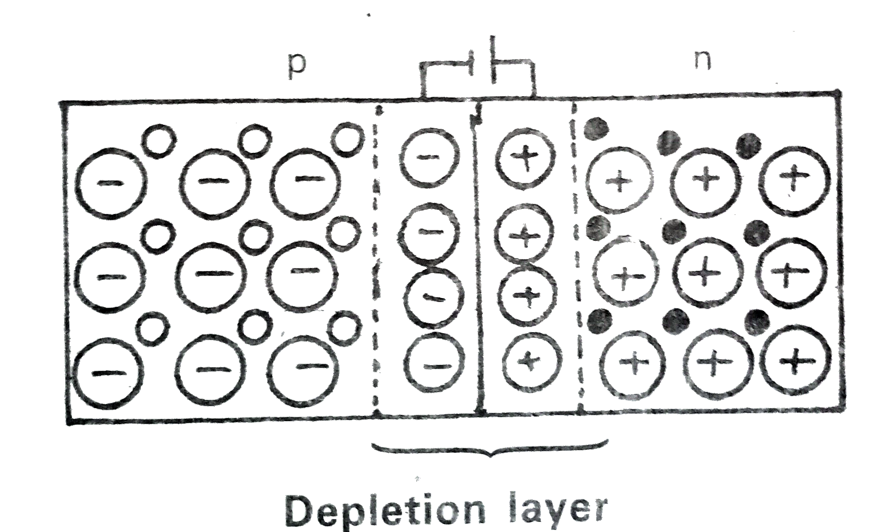
When p-n junction is formed, the free electron on n-side diffuse over to p-side , they combine with holes and become neutral.Similarly holeson p-side diffuse over to n-side and combine with electrons become neutral.
This results in a narrow region formed on either side of the junction.This region is called depletion laer.Depletion layer is free from charge carriers.
The n-type material near the junction becomes positively charged due to immobile donor ions and p-type material becomes negatively charged due to immobile acceptor ions. This creats an electric field near the junction directed from n-region to p-region and causesa potential barrier.
The potential barrier stops further diffusion of holes and electrons across the junction. The value of the potential barrier depends upon the nature of the crystal, its temperature and the amount of dopoing.

Topper's Solved these Questions
- SEMICONDUCTOR ELECTRONICS : MATERIALS , DEVICES , AND SIMPLE CIRCUITS BOOK - VIKRAM PUBLICATION ( ANDHRA PUBLICATION)CHAPTER - SEMICONDUCTOR ELECTRONICS : MATERIALS , DEVICES , AND SIMPLE CIRCUITS EXERCISE - LONG ANSWER QUESTIONS
7 Videos
- SEMICONDUCTOR ELECTRONICS : MATERIALS , DEVICES , AND SIMPLE CIRCUITS BOOK - VIKRAM PUBLICATION ( ANDHRA PUBLICATION)CHAPTER - SEMICONDUCTOR ELECTRONICS : MATERIALS , DEVICES , AND SIMPLE CIRCUITS EXERCISE - TEXTUAL EXERCISES
11 Videos
- SEMICONDUCTOR ELECTRONICS : MATERIALS , DEVICES , AND SIMPLE CIRCUITS BOOK - VIKRAM PUBLICATION ( ANDHRA PUBLICATION)CHAPTER - SEMICONDUCTOR ELECTRONICS : MATERIALS , DEVICES , AND SIMPLE CIRCUITS EXERCISE - VERY SHORT ANSWER QUESTIONS
14 Videos
- RAY OPTICAL AND INSTRUMENTSBOOK - VIKRAM PUBLICATION ( ANDHRA PUBLICATION)CHAPTER - RAY OPTICAL AND INSTRUMENTSEXERCISE - TEXTUAL EXERCISES
60 Videos
- TELANGANA MARCH-2019BOOK - VIKRAM PUBLICATION ( ANDHRA PUBLICATION)CHAPTER - TELANGANA MARCH-2019EXERCISE - SECTION -B
5 Videos
Similar Questions
What is a junction diode ? Explain the formation of depletion region at the junction. Explain the variation of depletion region in forward and reverse-biased condition.
View SolutionIn an n-type silicon, which of the following statement is true :
(a) Electrons are majority carriers are trivalent atoms are the dopants.
(b) Electrons are minority carriers and pentavalent atoms are the dopants.
(c ) Holes are minority carriers and pentavalent atoms are the dopants.
(d ) Holes are majority carriers and trivalent atoms are the dopants.
View SolutionWhat is an n-type semiconductor ? What are the majority and minority charge carriers in it?
View SolutionA small candal, 2.5 cm in size is placed at 27 cm in front of a concave mirror of radius of curvature 36 cm. At wht distance from the mirror should a screen be placed in order to obtain a sharp image ? Describe the nature and size of the image. If the candale is moved closer to the mirror, how would the screen have to be moved ?
View SolutionExplain the formation of Mirage .
View SolutionBarrier potential of a p-n junction diode does not depend on
View SolutionIn P−N junction, the barrier potential offerse resistance to
View SolutionWhat is p-n junction? How is a p-n junction made? How potential barrier is caused in it.
View SolutionThe barrier potential in a P-N junction is maximum in
View SolutionIn a p-n junction , the barrier potential offers resistance to
View SolutionBarrier potential of a p-n junction diode does not depent on
View SolutionIn forward bias in a p-n junction, the potential barrier
View SolutionBarrier potential of a p−n junction diode does not depend on
View SolutionIn forward bias in a p-n junction, the potential barrier
View SolutionHow does the effective junction potential barrier change when a p-n junction is reverse biased ?
View Solution
