Explain hole conduction in intrinsic semiconductors. Solution in Telugu
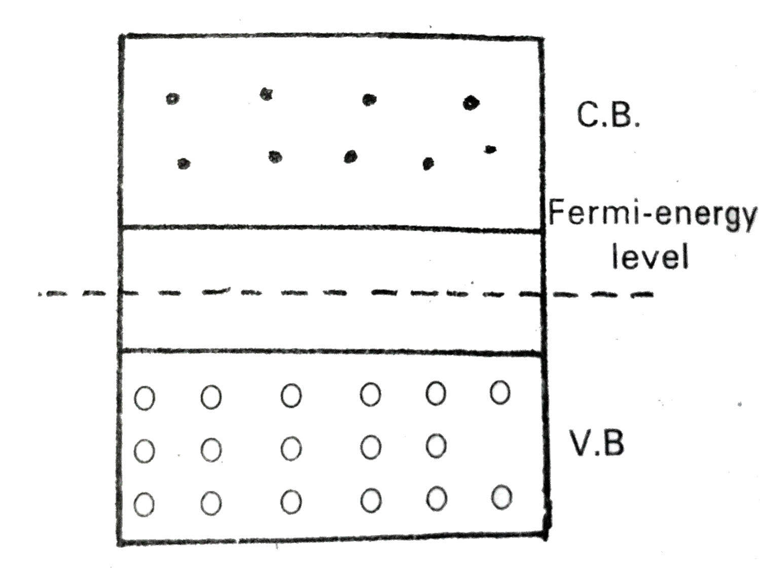
Pure semiconductors are called intrinsic semiconductors.At low temperature, velency band is filled with electrons and conduction band is empty. Hence it acts as an insulator at low temperature.
As temperature increases electrons in valence band get energy and jumps into the conduction band crossing the forbidden band. At their places in the valency banda vacancy is created.
This vacancy of electron in the valency band is called a hole.Hole has positivecharge and move only in the valency band, giving hole current.
In this Fermi-energy level will be at the middle of the forbidden band.

Topper's Solved these Questions
- SEMICONDUCTOR ELECTRONICS : MATERIALS , DEVICES , AND SIMPLE CIRCUITS Book:VIKRAM PUBLICATION ( ANDHRA PUBLICATION)Chapter:SEMICONDUCTOR ELECTRONICS : MATERIALS , DEVICES , AND SIMPLE CIRCUITS Exercise:LONG ANSWER QUESTIONS
Explore 7 Videos
- SEMICONDUCTOR ELECTRONICS : MATERIALS , DEVICES , AND SIMPLE CIRCUITS Book:VIKRAM PUBLICATION ( ANDHRA PUBLICATION)Chapter:SEMICONDUCTOR ELECTRONICS : MATERIALS , DEVICES , AND SIMPLE CIRCUITS Exercise:TEXTUAL EXERCISES
Explore 11 Videos
- SEMICONDUCTOR ELECTRONICS : MATERIALS , DEVICES , AND SIMPLE CIRCUITS Book:VIKRAM PUBLICATION ( ANDHRA PUBLICATION)Chapter:SEMICONDUCTOR ELECTRONICS : MATERIALS , DEVICES , AND SIMPLE CIRCUITS Exercise:VERY SHORT ANSWER QUESTIONS
Explore 14 Videos
- RAY OPTICAL AND INSTRUMENTSBook:VIKRAM PUBLICATION ( ANDHRA PUBLICATION)Chapter:RAY OPTICAL AND INSTRUMENTSExercise:TEXTUAL EXERCISES
Explore 60 Videos
- TELANGANA MARCH-2019Book:VIKRAM PUBLICATION ( ANDHRA PUBLICATION)Chapter:TELANGANA MARCH-2019Exercise:SECTION -B
Explore 5 Videos
Similar Questions
What is a junction diode ? Explain the formation of depletion region at the junction. Explain the variation of depletion region in forward and reverse-biased condition.
View SolutionIn an n-type silicon, which of the following statement is true :
(a) Electrons are majority carriers are trivalent atoms are the dopants.
(b) Electrons are minority carriers and pentavalent atoms are the dopants.
(c ) Holes are minority carriers and pentavalent atoms are the dopants.
(d ) Holes are majority carriers and trivalent atoms are the dopants.
View SolutionWhat is an n-type semiconductor ? What are the majority and minority charge carriers in it?
View SolutionA small candal, 2.5 cm in size is placed at 27 cm in front of a concave mirror of radius of curvature 36 cm. At wht distance from the mirror should a screen be placed in order to obtain a sharp image ? Describe the nature and size of the image. If the candale is moved closer to the mirror, how would the screen have to be moved ?
View SolutionExplain the formation of Mirage .
View SolutionLets npand ne be the number of holes and conduction electrons in an intrinsic semiconductor.
View SolutionWhen on impurity is doped into an intrinsic semiconductor, the conductivity of the semiconductor
View SolutionWith increase in temperature in an intrinsic semiconductor the ration of conduction electrons and holes is
View SolutionIn intrinsic semiconductor conductivity is
View SolutionIn intrinsic semiconductor conductivity is due to.
View SolutionThe ratio of number of holes and number of conduction electrons in an intrinsic semiconductor is
View Solutionएक नैज अर्धचालक (intrinsic semiconductor ) में होल (holes ) और चालन इलेक्ट्रॉनों की संख्याओं का अनुपात क्या होता है ?
View SolutionIn an intrinsic semiconductor at room temperature, number of electrons and holes are
View SolutionGive the ratio of the number of holes and the number of conduction electrons in an intrinsic semiconductor.
View SolutionHow is the conductivity of an intrinsic semiconductor be increased ?
View Solution

