Complete Solutions to PRACTICE PROBLEMS of chapter SEMICONDUCTOR ELECTRONICS METERIALS DEVICES AND SIMPLE CIRCUITS of Class 12 book with complete answers and questions
| Class 12 | PHYSICS |
| Chapter | SEMICONDUCTOR ELECTRONICS METERIALS DEVICES AND SIMPLE CIRCUITS |
| MODERN PUBLICATION | PRACTICE PROBLEMS |
| Number Of Questions | 26 |
| Academic Year | 2023-24 |
A pure semiconductor of volume `3.5 xx10^(-7) m^(3)` contains `5xx10^(20)` conduction electrons per `m^(3)` determine the number of holes present in it
View SolutionThe mean free path of conduction electron in a metallic block is `5xx10^(-6)` m the block is placed in an electric field of `5xx10^(+7) v m^(-1)` calculate the energy of the conduction electron in the block
View SolutionSuppose a pure Si-crystal has `5xx10^(28) "atoms" m^(-3)`. It is doped by 1 ppm concentration of pentavalent As. Calculate the number of electrons and holes. Give that `n_(i)=1.5xx10^(16)m^(-3)`.
View SolutionIn pure silicon semiconductor having same electron and hole concentration of `1.5 xx 10^(16)` the hole density is increased to 1.5 times on doping calculate the electron density in silicon after doping
View SolutionA semiconductor has equal electron and hole concentration of `6xx10^(8) m^(-3)` on doping with certain impurity electron concentration increases to `9xx10^(-12)` m calculate the new hole concentration
View SolutionThe separation between conduction band of electromagnetic radiation required to generate an electron hole pair in ti
View SolutionThe fobbidden gap in an ntype semiconductor is 4 me v so that the electrons are just able to enter the coduction band
View SolutionA type semiconductor sample has electron and hole concentration of `1.6 xx 10^(19)` the electron and hole mobility in the sample is `1.2 m^(2) v^(-1) s^(-1)` and 0.001 `m^(2)v^(-1) s^(-1)` respectively calculate the value of resistivity of the sample
View SolutionThe value of forward current in ap-n junction at 0.1 V is `1.04 xx10^(-2)` A calculate the reverse saturation current of the diode at 300 k kuse bottzmann's k =`1.4xx10^(-23)j K^(-1)` and exp (3.80)=44.7011
View SolutionThe values of v and I for silicon diode is given as follows

Using the data calculate the forward and reverse bias resistance of silicon diode
View SolutionVoltage drop across a p-n junction in forward bias is 0.5 V a battery of 2V is connected across the p-n junction such that the maximum current does not exceed 10 mA calculate the value of resistance to be connected across the diode
View SolutionA p-n junction diode in forward bias is connected to a battery of 4 V and a resistance of 80 `omega` as shown in the ajoining determine the maximum current in the circuit barrier potential of p-n diode is 0.2 V

View SolutionTwo diodes with internal resistance of 20 `omega` each are used in a full wave rectifier determine the mean load current and rms value of load current if load resistance of 800 `omega` given rms value of secondary voltage is 40 V
View SolutionThe rms value of input voltage in a full wave rectifier is 12 V determine the output voltage if a step up a transformer with ratio 1:2 is used
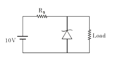
View SolutionIn a Zener regulated power supply a Zener diode with `V_(Z) = 6.0 V` is used for regulation. The load current is to be 4.0 mA and the unregulated input is 10.0 V. What should be the value of series resistor `R_(S)` ? Choose zener current to be 20 mA.

View SolutionA 10V of zener diode is connected in series to a resistance across a power supply of 50 V calculate the minimum value of resistance required such that the zener current is 25 mA
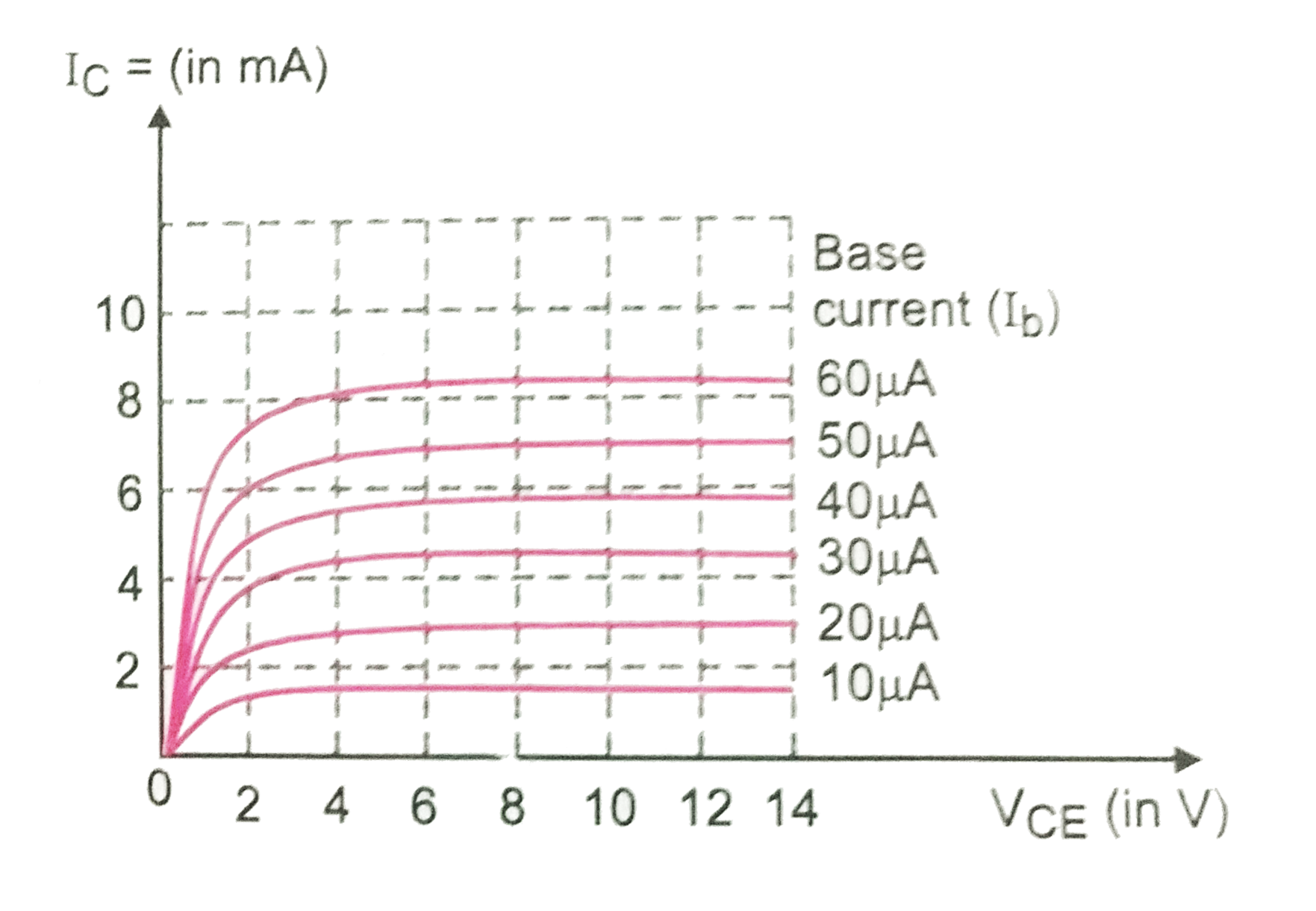
View SolutionFrom the output characteristics of common emitter circuit shown in Fig., calculate the value of `beta_(ac)` and `beta_(dc)` of the transistor when `V_(cE)` is `10 V` and `I_c =4.0mA`.

View SolutionIn a common emitter transistor the potential drop across the collector is found to be 2 v claculate the emitter current if value of collector resistance is 2 `komega` the dc gain of transistor is 40
View SolutionIn a common base transistor the value of load resistance in output and input circuit is 500 `komega` and 300 `omega` respectively calculate the voltage gain and power gain if value of current gain is 0.90
View SolutionIn a semiconductor transistor there is change in collector current of 8.2 mA with change of 8.29 mA in emitter current calculate the change in base current that produces same change in collector current
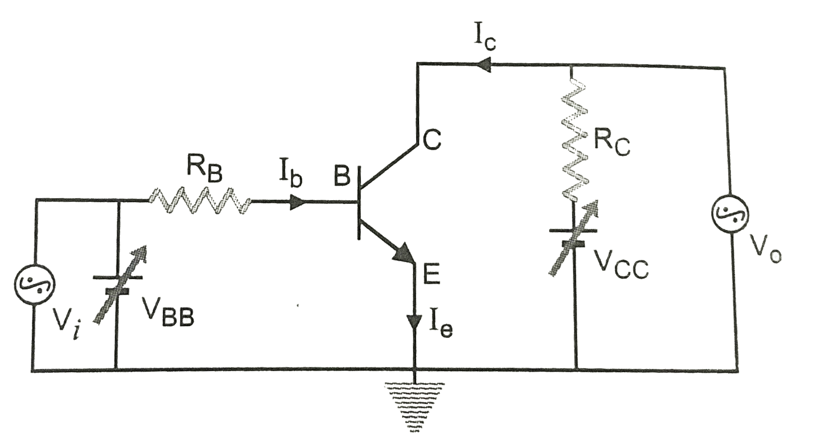
View SolutionIn common emitter transistor as shown in Fig., the `V_(BB)` supply can be varied from 0 V to 5.0V. The Si. Transistor has `beta_(ac)=250` and `R_(B)=100kOmega, R_(c)=1k Omega,V_(C C)=5.0V`. Assume that when the transistor is saturated, `V_(CE)=0V` and `V_(BE)=0.8V`. Calculate the minimum base current, for which the transistor will reach saturation. Hence, determine `V_(i)` when the transistor is 'switched on' find ranges of `V_(i)` for which the transistor is switched off and switched on.

View SolutionFor a CE transistor amplifier the audio signal voltage across the collector resistance of 2.0 `komega` is 2.0 V suppose the current amplification factor of the transistor is 100 what should be the value of `R_(B)` in series with `V_(BB)` 10 times the signal current also calculate the DC drop across the collector resistance
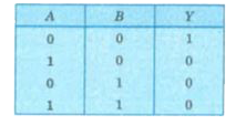
View SolutionWhich gate is represented by the given truth table

View SolutionYou are given a circuit below write its truth table hence identify the logic operation carried out by the circuit draw the logic symbol of the gate it corresponds to

View SolutionIdentify the logic gates marked P and Q in the circuit Fig. Write the truth table for this combination.

View SolutionWrite the truth table for the given combination of gates

View Solution
PRACTICE PROBLEMS questions and complete solutions for chapter SEMICONDUCTOR ELECTRONICS METERIALS DEVICES AND SIMPLE CIRCUITS of MODERN PUBLISHERS PHYSICS (HINGLISH) of Class 12
All Exercises from MODERN PUBLICATION Class 12 PHYSICS SEMICONDUCTOR ELECTRONICS METERIALS DEVICES AND SIMPLE CIRCUITS
- CHAPTER PRACTICE TEST FOR BOARD EXAMINATION
- COMPETION FILE (MULTIPLE CHOICE QUESTIONS WITH ONLY ONE CORRECT ANSWER)
- COMPETION FILE (ASSERTION REASON TYPE QUESTIONS )
- COMPETION FILE (INTEGER TYPE QUESTIONS)
- COMPETION FILE (JEE(MAIN) & OTHER STATE BOARDS FOR ENGINEERING ENTRANCE )
- COMPETION FILE (MATCHING TYPE QUESTIONS )
- COMPETION FILE (MATRIX MATCH TYPE QUESTIONS)
- COMPETION FILE (NCERT EXEMPLAR PROBLEMS :MULTIPLE CHOICE QUESTION TYPE -I)
- COMPETION FILE (NCERT EXEMPLAR PROBLEMS :MULTIPLE CHOICE QUESTION TYPE -II)
- COMPETION FILE( MULTIPLE CHOICE QUESTIONS )
- CONCEPUAL QUESTIONS
- HIGER ORDER THINKING SKILLS & ADVANCED LEVEL
- NCERT FILE SOLVED (TEXT BOOK EXERCISES )
- PRACTICE PROBLEMS
- REVISION EXERCISES (ADDITOINAL QUESTION)
- REVISION EXERCISES (NUMERICAL PROBLEMS )
- REVISION EXERCISES (SHORT ANSWER QUESTION )
- REVISION EXERCISES (VERY SHORT ANSWER QUESTION)
- REVISION EXERCISES( LONG ANSWER QUESTIONS)
- REVISION EXERCISES(FILL IN THE BLANKS )
- SOLVED EXAMPLES
- TOUGH & TRICKY PROBLEMS