Complete Solutions to CONCEPUAL QUESTIONS of chapter SEMICONDUCTOR ELECTRONICS METERIALS DEVICES AND SIMPLE CIRCUITS of Class 12 book with complete answers and questions
| Class 12 | PHYSICS |
| Chapter | SEMICONDUCTOR ELECTRONICS METERIALS DEVICES AND SIMPLE CIRCUITS |
| MODERN PUBLICATION | CONCEPUAL QUESTIONS |
| Number Of Questions | 37 |
| Academic Year | 2023-24 |
C, Si and Ge have same lattice structure. Why is C insulator,
while Si and Ge intrinsic semiconductors ?
View SolutionWhat type of inter atomic bonding is there in semiconductors
View SolutionWhy doping is done in semiconductor?
View SolutionCan we take one slab of p - type semiconductor and physically
join it to another n - type semiconductor to get p - n junction?
View SolutionHow does the width of the depletion layer of a p-n junction diode change with decrease in reverse bias?
View SolutionIntrinsic and extrinsic semiconductors .
View Solutionp-type and n-type semiconductors .
View SolutionA p - type semiconductor crystal is electrically neutral although it has larger number of holes explain
View SolutionIn a semiconductor energy gap between the impurites level and conduction band is 1 me V is it an n type or p type of semiconductor
View SolutionOut of electron and hole, which one has higher mobility and Why?
View SolutionHow does the forbidden energy gap of an intrinsic semiconductor vary with the increase in temperature
View SolutionAn intrinsic semiconductor is doped with boron how will the energy gap change in semiconductor
View SolutionAn intrinsic semiconductor is doped with arsenic how will the energy gap change in semiconductor
View SolutionWhat will happen to the conductivity of a semiconductor on passing large currents through it
View SolutionGraphically represent the variatin of resistivity of carbon with temperture
View SolutionWhy si and gaas are preferred material for solar cells
View SolutionThe resistance of p-n junction is low when forward biased and is high when reverse biased. Explain.
View SolutionA p n junction diode is connected to a battery of 2 v and a resistance of 8 ohm as shown in figure calculate the current passing through the resistor
View SolutionA p -n junctin diode is connected to a battery of 2 V and a resistance as shownin the adjoining calculate the curernt passing through the resistor

View SolutionA half wave rectifier provides DC output power of 30 W when 100 W AC power is supplied to it what will be the rectification efficiency and power efficiency
View SolutionHow can we use a diode as a switch
View SolutionHow can we increase the intensity of an LED
View SolutionIn a transistor base is made thin and doped with little impurity atoms. Why?
View SolutionHow will the current in the transistor change with the increase in temperature
View SolutionExplain, why the input resistance of a transistor is low and output resistance is high.
View SolutionTransistor also works bidirectinaly commment
View SolutionIn a transistor both emitter base jucntion and colector base junction are reverse biased how will the concentration of charge carrier across the each junction change
View SolutionIf the base region of a transistor is made large, as compared to a usual transistor, how does it affect (i) the collector current and (ii) current gain of this transistor.
View SolutionIn the given circuit diagram, a voltmeter 'V' is connected across a lamp 'L'. How would (i) the brightness of the lamp and (ii) voltmeter reading 'V' be affected, if the value of resistance 'R' is decreased ? Justify your answer.
View SolutionHow are analogue and digital signals different
View SolutionDiscuss how a NOT gate is realised using NAND gates.
View SolutionRealise the formation of AND gate using NAND gate
View SolutionRealise the formation of OR gate from NAND gate
View Solution

View SolutionNAND gate is also known as digital building block explain
View SolutionArrange two NAND gates and one OR gate such that the combination obtained acts as the NAND gate only
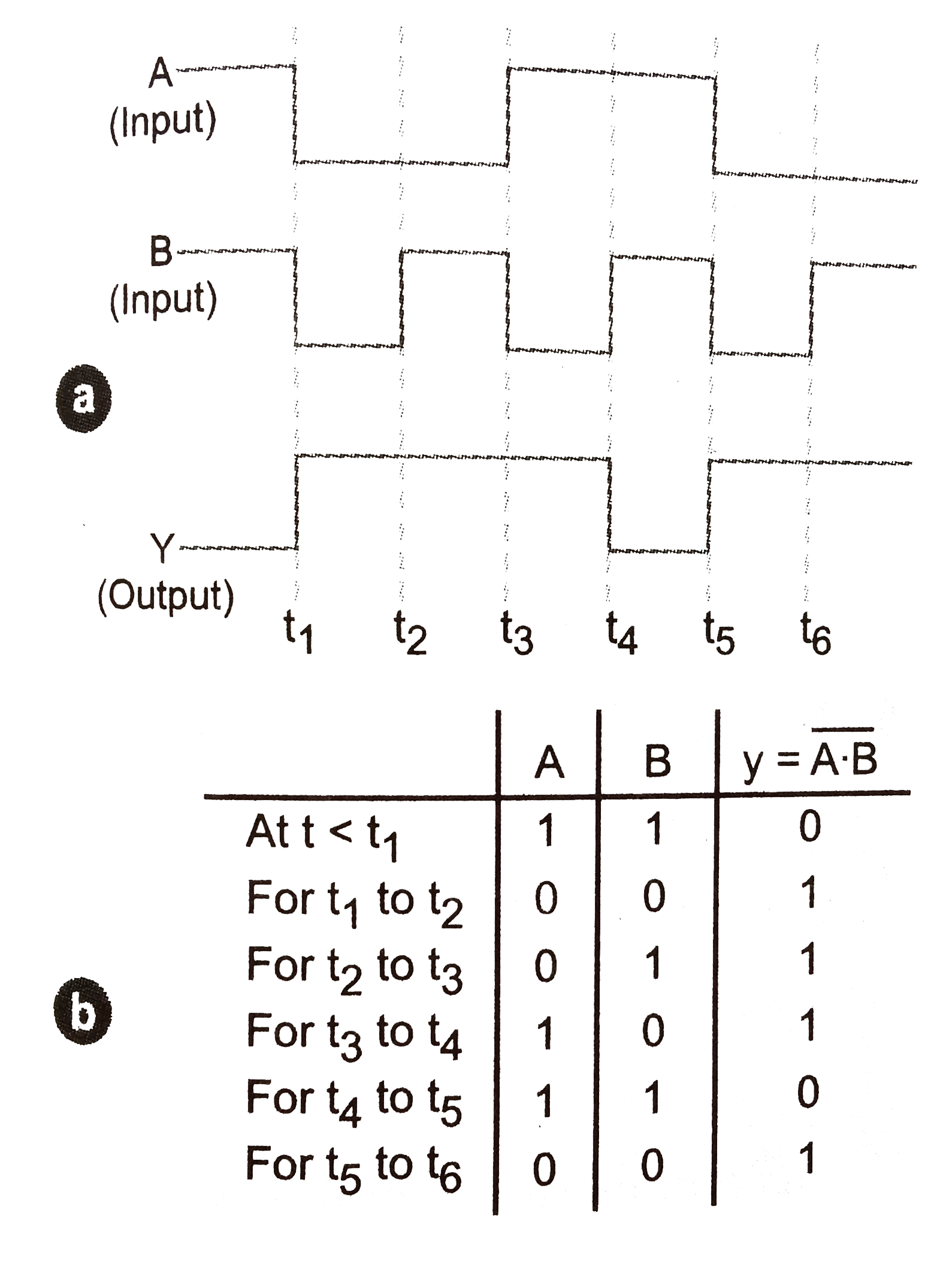
View SolutionThe following Fig. shows the input waveforms (A,B) and the output waveform (y) of a gate. Identify the gate and write its truth table.

View Solution
CONCEPUAL QUESTIONS questions and complete solutions for chapter SEMICONDUCTOR ELECTRONICS METERIALS DEVICES AND SIMPLE CIRCUITS of MODERN PUBLISHERS PHYSICS (HINGLISH) of Class 12
All Exercises from MODERN PUBLICATION Class 12 PHYSICS SEMICONDUCTOR ELECTRONICS METERIALS DEVICES AND SIMPLE CIRCUITS
- CHAPTER PRACTICE TEST FOR BOARD EXAMINATION
- COMPETION FILE (MULTIPLE CHOICE QUESTIONS WITH ONLY ONE CORRECT ANSWER)
- COMPETION FILE (ASSERTION REASON TYPE QUESTIONS )
- COMPETION FILE (INTEGER TYPE QUESTIONS)
- COMPETION FILE (JEE(MAIN) & OTHER STATE BOARDS FOR ENGINEERING ENTRANCE )
- COMPETION FILE (MATCHING TYPE QUESTIONS )
- COMPETION FILE (MATRIX MATCH TYPE QUESTIONS)
- COMPETION FILE (NCERT EXEMPLAR PROBLEMS :MULTIPLE CHOICE QUESTION TYPE -I)
- COMPETION FILE (NCERT EXEMPLAR PROBLEMS :MULTIPLE CHOICE QUESTION TYPE -II)
- COMPETION FILE( MULTIPLE CHOICE QUESTIONS )
- CONCEPUAL QUESTIONS
- HIGER ORDER THINKING SKILLS & ADVANCED LEVEL
- NCERT FILE SOLVED (TEXT BOOK EXERCISES )
- PRACTICE PROBLEMS
- REVISION EXERCISES (ADDITOINAL QUESTION)
- REVISION EXERCISES (NUMERICAL PROBLEMS )
- REVISION EXERCISES (SHORT ANSWER QUESTION )
- REVISION EXERCISES (VERY SHORT ANSWER QUESTION)
- REVISION EXERCISES( LONG ANSWER QUESTIONS)
- REVISION EXERCISES(FILL IN THE BLANKS )
- SOLVED EXAMPLES
- TOUGH & TRICKY PROBLEMS