Complete Solutions to COMPETION FILE (MULTIPLE CHOICE QUESTIONS WITH ONLY ONE CORRECT ANSWER) of chapter SEMICONDUCTOR ELECTRONICS METERIALS DEVICES AND SIMPLE CIRCUITS of Class 12 book with complete answers and questions
| Class 12 | PHYSICS |
| Chapter | SEMICONDUCTOR ELECTRONICS METERIALS DEVICES AND SIMPLE CIRCUITS |
| MODERN PUBLICATION | COMPETION FILE (MULTIPLE CHOICE QUESTIONS WITH ONLY ONE CORRECT ANSWER) |
| Number Of Questions | 51 |
| Academic Year | 2023-24 |
The electrical conductivity of semicondutor increases when electromagnetic radiation of wavelength shorter than 29800 Å is incident on it. The band gap for the semiconductor is
View SolutionA half wave rectifer circuit is constracted using a p-n junction dode D load resistacne R and AC source as shown below
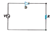
The current thourgh R varies as
View SolutionIn the current versus voltage characteristics of a diode minimum current of 1 mA is required for the knee voltage to be is connected in a cirucit the minimum value of R so that the voltage is above knee point is
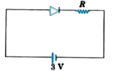
View SolutionAtoms of phosphorus aresnic indium and bismuth are used for doping pure semicondluctors to produce p type or n type semiconductors p tyhpe semocnductor
View SolutionThe current gain of a tramnsistor is 0.9 for common base configuration if the change in emitter current is 8 mA the change in base current is
View SolutionThe dominant mechanisms for motion of charge carriers in forward and reverse biased silicon `P-N` junction are
View SolutionTwo diodes `D_(1)` and `D_(2)` each with forward resistance of 50 `omega` and infinite backward resistance are connected as the current througjh thej 150 `omega` resistance is
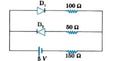
View SolutionFour diodes are connected in the adjoining in order for the circuit toact as a full wave DC output are connected and obtained respectively across

View SolutionI-V characteristics of four semiconductor devices are in graphs (i) ,(ii) (iii) and (iv) the characteristics of zener diode and solar cell are show correctly in :
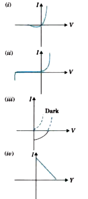
View SolutionIn which of the following connections the diode is forward biased
View Solution
The above combination of gates produces a
View SolutionGe and Si diods in the circuit belwo conduct at 0.3 V and 0.7 V respectiveluy if the connection of Ge diode in now reversed the change in value of V is

View SolutionInput A,B,C,D are given to a gate and y is the oputput obtained from we can see that the gate is

View SolutionSi diode used in the circuit shhas a constant voltage drop of a maximum power rating resistance R to obtain maixmum current is
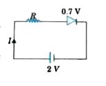
View SolutionA transistor with a current gian of `beta=50` is used as an amplifier if the voltage across the load resistance `R_(c ) =5 komega` in the collectro cirucit is 2.5 V the base current is
View SolutionAn n-p-n tansistor circuit is show below
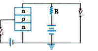
The arrangement represent a
View SolutionAt a plate potential of 150 V the palte current in a diode is 8 mA under space charge limited conditions if the plate potential is changed to 300 V the plate current is
View SolutionIn the circuit given below the p-n junction diode is ideal with negligible forward resistance and infinite backward resistance the current in the circuit is
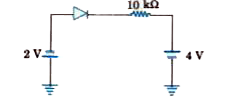
View SolutionIn which of the following ciruict the potiential drop across the two p-n juctins are equal take all p-n junctions to be identical

View SolutionA piece of copper and anotehr piece of silicon are cooled down to 80 k from room temperatrue then the resistance of
View SolutionA `Ge` specimen is dopped with `Al`. The concentration of acceptor atoms is `~10^(21) at oms//m^(3)`. Given that the intrinsic concentration of electron hole pairs is `~10^(19)//m^(3)`, the concentration of electron in the speciman is
View SolutionIn the cirucit given below the knee voltage for both the diodes is 0.5 v the current shupplied by the battery is
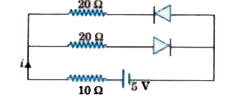
View SolutionThe contribution in the total current flowing through a semiconductor due to electrons and holes are `3/ 5` and `2/ 5` respectively. If the drift velocity of electrons is 2 times that of holes at this temperature, then the ratio of concentration of electrons and holes is
View SolutionIn the curcuit given below `D_(1)` and `D_(2)` are two identicall diodes and V is a sinusoidal voltage source the voltage drop across the resistance `R_(L)`

View SolutionFor the combination of gates given below the output y is high if

View SolutionThe base of a transistor is kept very thin and lightly doped as compared to the emitter and collector region so that
View SolutionA transistor -oscillator using a resonant circuit with an inductor `L` (of negligible resistance) and a capacitor `C` in series produce oscillations of frequency `f`. If `L` is doubled and `C` is changed to `4C`, the frequency will be
View SolutionFor a p-type semiconductor, which of the following statements is true?
View SolutionThe correct booleon operation represented by the circuit diagram drawn is
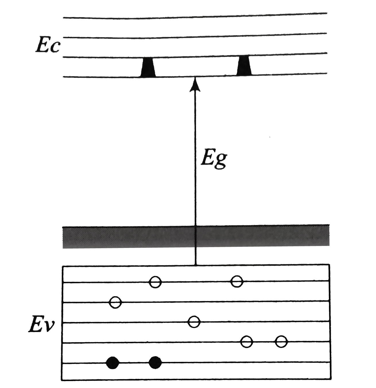
View SolutionIn the energy band diagram of a material shown below, the open circles and filled circles denote holes and electrons respectively. The material is a/an
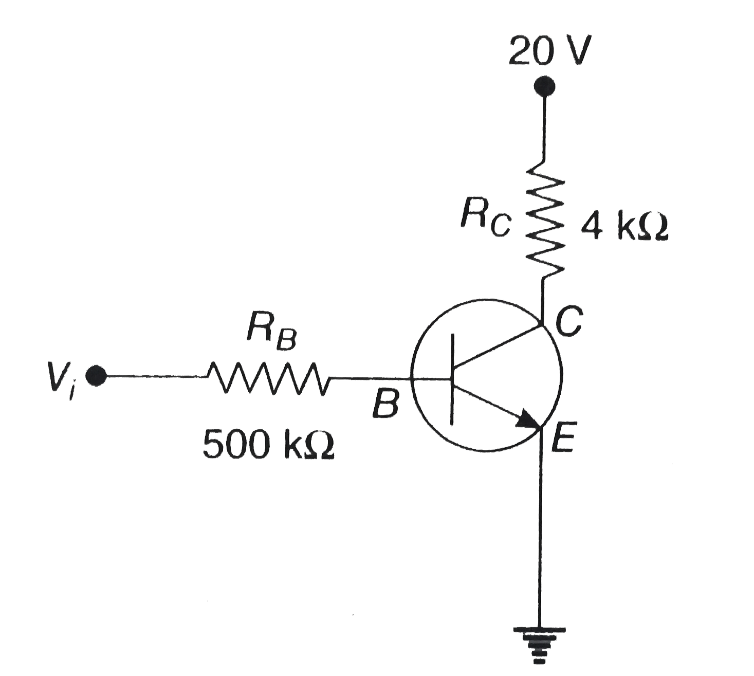
View SolutionIn the circuit shown in the figure, the input voltage `V_(i)` is `20V,V_(BE)=0` and `V_(CE)=0`. The values of `I_(B),I_(C)` and `beta` are given by:
View SolutionIn a `p-n` junction diode, change in temperature due to heating
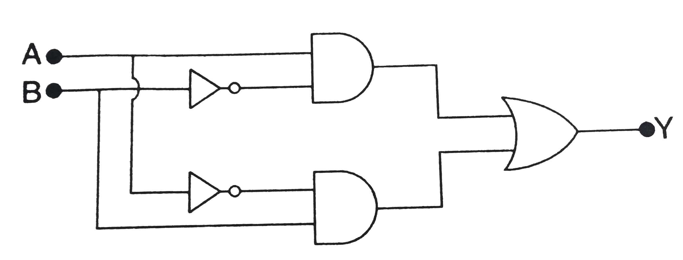
View SolutionIn the combination of the following gates the output `Y` can be written in terms of inputs `A` and `B` as:
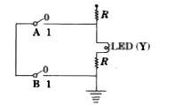
View SolutionA light emitting diode `(LED)` has a voltage drop of `2V` across it and passes a current of `10 mA`. When it operates with a `6V` battery through a limiting resistor `R`. The value of `R` is
View SolutionA `p-n` photodiode is made of a material with a band gap of `2.0 eV`. The minimum frequency of the radiation that can be absorbed by the material is nearly
View SolutionA `p-n` photodiode is fabricated from a semiconductor with a band gap of `2.5 eV`. It can detect a signal of wavelength
View SolutionA transistor is operated in common emitter configuration at `V_(c)=2 V` such that a change in the base current from `100 muA` to `200 muA` produces a change in the collector current from `5 mA` to `10 mA`. The current gain is
View SolutionA common emitter amplifier has a voltage gain of 50, an input impedance of `100Omega` and an output impedance of 200 `Omega`. The power gain of the amplifier is :-
View SolutionIf a small amount of antimony is added to germanium crystal
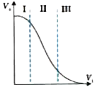
View SolutionTransfer characteristics vs input volage for a base biased transistor in CE configuration for using transistor as a switch it is used
View Solution`C` and `Si` both have same lattice structure, having `4` bonding electrons in each. However, `C` is insulator whereas `Si` is intrinsic semiconductor. This is because
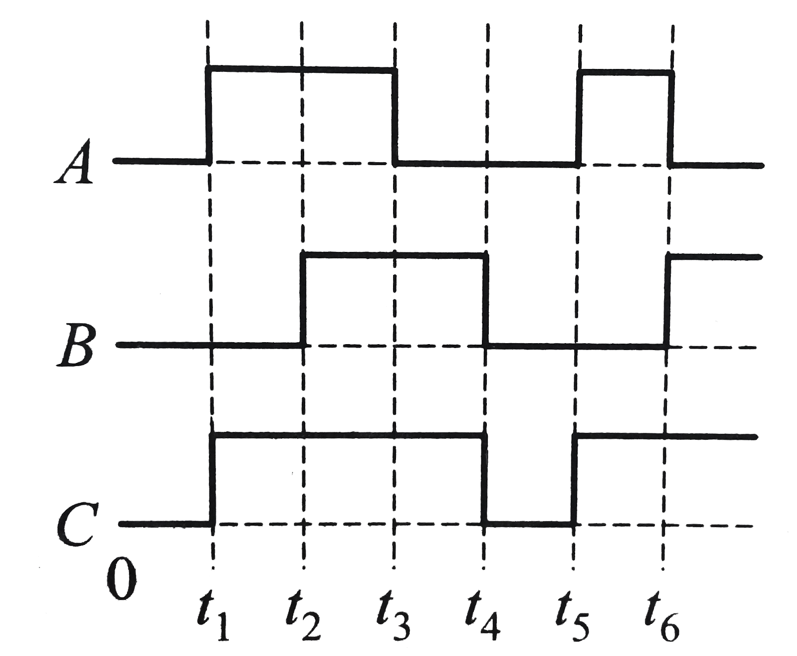
View SolutionThe figure shows a logic circuit with two inputs `A` and `B` and the output `C`. The voltage wave forms across `A,B` and `C` are as given. The logic circuit gate is
View SolutionIn a common emitter (CE) amplifier having a voltage gain G, the transistor used has transconductor 0.03 mho and current gain 25. If the above transistor is replaced with another one with transconductance 0.02 mho and current gain 20, the voltage gain will
View SolutionThe ouptu x of the logic circuit will be

View SolutionThe given graph represents V-I characteristic for a semiconductor device which of the following statement is correct

View SolutionThe barrier potential of a p-n junction depends on : (a) type of semiconductor material (b) amount of doping (c) temperature.
Which is one of the following is correct?
View SolutionConsider the juction diode as ideal the value of current flowing through AB is

View SolutionA n-p-n transisitor is connected in common emitter configuration in a given amplifier. A load resistance of `800 Omega` is connected in the collector circuit and the voltage drop across it is `0.8 V`. If the current amplification factor is `0.96` and the input resistance of the circuits is `192 Omega`, the voltage gain and the power gain of the amplifier will respectively be
View SolutionTo get output 1 for the following circuit the correct choice for the input is
f
View SolutionThe given electrical network is equivalent to

View SolutionIn a common emitter transistor amplifier the audio signal voltage across the collector is `3 V`. The resistance of collector is `3 kOmega`. If current gain is `100` and the base resistance is `2 kOmega`, the voltage and power gain of the amlifier is :
View Solution
COMPETION FILE (MULTIPLE CHOICE QUESTIONS WITH ONLY ONE CORRECT ANSWER) questions and complete solutions for chapter SEMICONDUCTOR ELECTRONICS METERIALS DEVICES AND SIMPLE CIRCUITS of MODERN PUBLISHERS PHYSICS (HINGLISH) of Class 12
All Exercises from MODERN PUBLICATION Class 12 PHYSICS SEMICONDUCTOR ELECTRONICS METERIALS DEVICES AND SIMPLE CIRCUITS
- CHAPTER PRACTICE TEST FOR BOARD EXAMINATION
- COMPETION FILE (MULTIPLE CHOICE QUESTIONS WITH ONLY ONE CORRECT ANSWER)
- COMPETION FILE (ASSERTION REASON TYPE QUESTIONS )
- COMPETION FILE (INTEGER TYPE QUESTIONS)
- COMPETION FILE (JEE(MAIN) & OTHER STATE BOARDS FOR ENGINEERING ENTRANCE )
- COMPETION FILE (MATCHING TYPE QUESTIONS )
- COMPETION FILE (MATRIX MATCH TYPE QUESTIONS)
- COMPETION FILE (NCERT EXEMPLAR PROBLEMS :MULTIPLE CHOICE QUESTION TYPE -I)
- COMPETION FILE (NCERT EXEMPLAR PROBLEMS :MULTIPLE CHOICE QUESTION TYPE -II)
- COMPETION FILE( MULTIPLE CHOICE QUESTIONS )
- CONCEPUAL QUESTIONS
- HIGER ORDER THINKING SKILLS & ADVANCED LEVEL
- NCERT FILE SOLVED (TEXT BOOK EXERCISES )
- PRACTICE PROBLEMS
- REVISION EXERCISES (ADDITOINAL QUESTION)
- REVISION EXERCISES (NUMERICAL PROBLEMS )
- REVISION EXERCISES (SHORT ANSWER QUESTION )
- REVISION EXERCISES (VERY SHORT ANSWER QUESTION)
- REVISION EXERCISES( LONG ANSWER QUESTIONS)
- REVISION EXERCISES(FILL IN THE BLANKS )
- SOLVED EXAMPLES
- TOUGH & TRICKY PROBLEMS