Complete Solutions to COMPETION FILE (JEE(MAIN) & OTHER STATE BOARDS FOR ENGINEERING ENTRANCE ) of chapter SEMICONDUCTOR ELECTRONICS METERIALS DEVICES AND SIMPLE CIRCUITS of Class 12 book with complete answers and questions
| Class 12 | PHYSICS |
| Chapter | SEMICONDUCTOR ELECTRONICS METERIALS DEVICES AND SIMPLE CIRCUITS |
| MODERN PUBLICATION | COMPETION FILE (JEE(MAIN) & OTHER STATE BOARDS FOR ENGINEERING ENTRANCE ) |
| Number Of Questions | 31 |
| Academic Year | 2023-24 |
In a common emitter configuration with suitable bias, it is given that `R_(L)` is theload resistance and `R_(BE)` is small signal dynamic resistance (iiput side). Then, volage gain, current gain and power gain are given , respectively, by :
`beta` is currentgain , `I_(B), I_(C)` and `I_(E)` are respectively base, collector and emitter currents.
View SolutionA common emitted amplifier circuit, built using an npn transistor, is shown in the figure. Its dc current gain is `250,R_(C)=1Komega` and `V_(C C)=10V`. What is the minimum base current for `V_(CE)` to reach saturation?
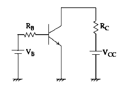
View SolutionAn NPN transistor is used in common emitter configuration as an amplifier with `1 k Omega` load resistance. Signal voltage of 10 mV is applied across the base-emitter. This produces a 3 mA change in the collector current and `15 mu A` change in the base current of the amplifier. The input resistance and voltage gain are:
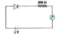
View SolutionThe reading of an ammeter for a silicon diode in the given circuit is
View Solutiona p -n juction (D) shown in the figure can act an a rectifier An alternatting current source (V) is connected in the circuit
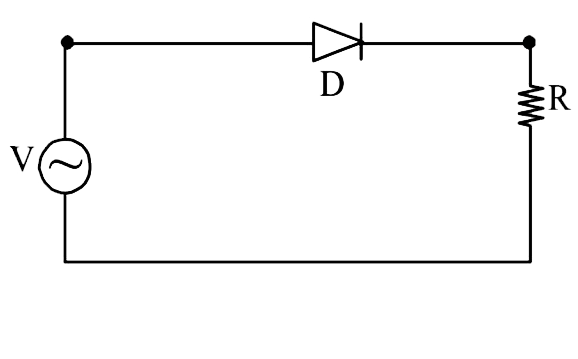
The corrent (I ) in the resistor® can be shown by :
View SolutionThe logic circuit show below has the input waveform A and B as shown pick out the correct output waveform

View SolutionThe combination of gates shown below yields

View SolutionThe output of an OR gate is connected to both the inputs of a NAND gate. The combination will serve as a
View SolutionIn the givne circuit the current through zener diode is

View SolutionThe `I-V` characteristic of an `LED` is.
View SolutionThe forward biased diode connection is
View SolutionThe currect voltage relation of diode is given by `1=(e^(1000 V//T)-1) mA`, where the applied voltage V is in volt and the temperature T is in degree Kelvin. If a student makes an error measuring `+-0.01 V` while measuring the current of `5 mA` at `300 K`, what will be error in the value of current in mA?
View SolutionA red LED emits light of 0.1 watt uniformaly around it. The amplitude of the electric field of the light at a distance of 1m from the diode is
View SolutionFor LEDs to emit light in visible region of electromagnetic light it should have energy band gap in the range of
View SolutionThe value of the resistor `R_(s)` needed in the DC voltage regulator circuit shown here equals

View SolutionA 2 V battery is connecte across AB the value of the current supplied by the battery when in one case battery positive terminal is connected to A and in other case when positive terminal of battery is connected to B will respectively be

View SolutionA zener diode is connecte to battery and a load The currents I ,`I_(z)` and `I_(L)` are respectively

View SolutionIn an unbiased p-n junction electrons diffuse from n region to p region because
View Solutionif `a,b,c,d`are inputs to a gate and `x` is its output , then as per the following time graph , the gate is :
d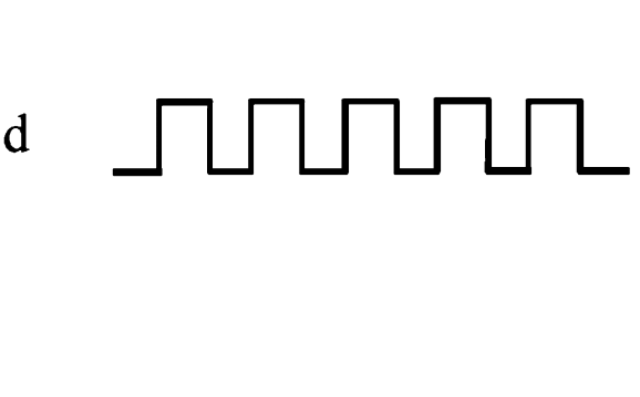
c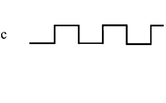
b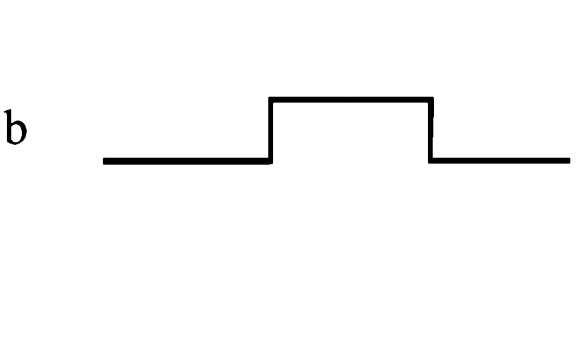 a
a
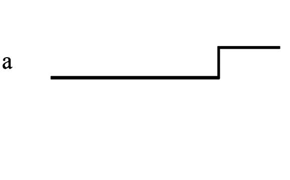 x
x
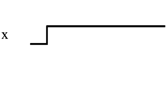
View SolutionIdentify the semiconductor devices whose characteristics are in the order (A),(b) (c ),(d)

View SolutionFor a common emiter configuration if `a` and `beta` have their usualy meaning , the incorrrect relationship between `a and beta` is :
View SolutionAn experiment is preformed to determine the `I-V` characteristics of a Zener diode, which has a protective resistance of `R = 100 Omega`, and maximum power of dissipation rating of 1 W. The minimum voltage range of the DC source in the circuit is :-
View SolutionAn unknown transistor needs to be identified as `npn` and `pnp` type. A multimeter, wilth `+ve` and `-ve` terminals is used to measure resistance between different terminals transistor. If terminal `2` is the base of the transistor then which of the following is correct for a `pnp` transistor?
View SolutionTo get an output of 1 from the circuit shown the input must be

View SolutionA realistic graph depiciting the variation of thhe reciprocal of input resistance in an in- put charcteristics measurement in a com- mon emitter transistor configuration is :
View SolutionThe ratio (R) of output resistance `r_0` and the input resistance r, in measurements of input and output charactersitics of a transistor is typically in the range :
View SolutionIdentify the gate and match A,B,Y in bracket to check

View SolutionAn n-p-n transistor has three leads A,B and C connecting B and C by moist fingers A to the positive lead of an ammeter and c to the negative lead of the ammeter one finds large deflection then a,b and c refer respectively to
View SolutionThe V-I characteristic of a diode is the ratio of forward to revese bias resistance is

View SolutionThe current gain for common emitter amplifier is 69. If the emitter current is `7.0 mA`, find (i) base current and (ii) collector current.
View SolutionIn a common emitter amplifier circuit using an n-p-n transistor, the phase difference between the input and the output voltages will be:-
View Solution
COMPETION FILE (JEE(MAIN) & OTHER STATE BOARDS FOR ENGINEERING ENTRANCE ) questions and complete solutions for chapter SEMICONDUCTOR ELECTRONICS METERIALS DEVICES AND SIMPLE CIRCUITS of MODERN PUBLISHERS PHYSICS (HINGLISH) of Class 12
All Exercises from MODERN PUBLICATION Class 12 PHYSICS SEMICONDUCTOR ELECTRONICS METERIALS DEVICES AND SIMPLE CIRCUITS
- CHAPTER PRACTICE TEST FOR BOARD EXAMINATION
- COMPETION FILE (MULTIPLE CHOICE QUESTIONS WITH ONLY ONE CORRECT ANSWER)
- COMPETION FILE (ASSERTION REASON TYPE QUESTIONS )
- COMPETION FILE (INTEGER TYPE QUESTIONS)
- COMPETION FILE (JEE(MAIN) & OTHER STATE BOARDS FOR ENGINEERING ENTRANCE )
- COMPETION FILE (MATCHING TYPE QUESTIONS )
- COMPETION FILE (MATRIX MATCH TYPE QUESTIONS)
- COMPETION FILE (NCERT EXEMPLAR PROBLEMS :MULTIPLE CHOICE QUESTION TYPE -I)
- COMPETION FILE (NCERT EXEMPLAR PROBLEMS :MULTIPLE CHOICE QUESTION TYPE -II)
- COMPETION FILE( MULTIPLE CHOICE QUESTIONS )
- CONCEPUAL QUESTIONS
- HIGER ORDER THINKING SKILLS & ADVANCED LEVEL
- NCERT FILE SOLVED (TEXT BOOK EXERCISES )
- PRACTICE PROBLEMS
- REVISION EXERCISES (ADDITOINAL QUESTION)
- REVISION EXERCISES (NUMERICAL PROBLEMS )
- REVISION EXERCISES (SHORT ANSWER QUESTION )
- REVISION EXERCISES (VERY SHORT ANSWER QUESTION)
- REVISION EXERCISES( LONG ANSWER QUESTIONS)
- REVISION EXERCISES(FILL IN THE BLANKS )
- SOLVED EXAMPLES
- TOUGH & TRICKY PROBLEMS