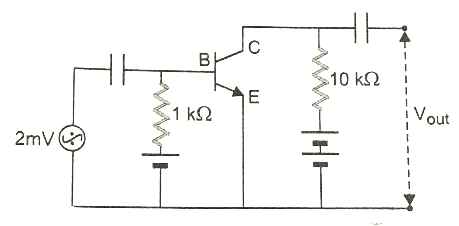
With the help of circuit diagram, explain the working of transistor as a common emitter amplifier.Solution in Punjabi
The Amplifier circuit using p-n-p transistor is shown in the following Figure. Figure shows that the base-emitted circuit is forward biased. Therefore the resistance in the input circuit in less. The collector-emitter circuit is output circuit and reverse biased. Therefore resistance in the output circuit is more. When no a.c input signal is applied, then the transistor works normally and Ie=Ib+Ic. When Ic flows through load resistance RL, then potential drop equal to ICRL will occur. Therefore output voltage is

Vo=VCE−ICRL ..(i)
When input a.c signal is applied, it will change emitter current Ie and hence collector current Ic. Therefore, from eqn (i), output voltage (Vo) will appear as amplifier voltage.
During positive half cycle of a.c., the forward voltage of emitter -base junction decreases. Due to this, emitter current (Ie) and hence collector current (Ic) also decrease. Therefore, voltage drop across RL i.e., ICRL will also decrease. Therefore, from eqn (i) output voltage increases. As the collector is connected to negative terminal of the battery, so increase in output voltage means the collector voltage becomes more negative i.e., the output voltage Vo will vary in negative sense and corresponding to positive half cycle of a.c. input, negative output half cycle will be obtained. During negative half-cycle of a.c. the forward voltage of emitter -base junction increases. Due to this, emitter current (Ie) and hence collector current (Io) also increase. Therefore, voltage drop across RL i.e., ICRL increases. Hence from eqn (i), the output voltage decreases. As the collector is connected to negative terminal of battery VCE, so decrease in output voltage means the output voltage becomes less negative i.e output voltage Vo will vary in positive sense and corresponding to negative half cycle of a.c input, positive output half cycle will be obtained. Hence, both input and output voltage are out of phase.
(i) A.C. current gain (β) It is the ratio of change in output current (ΔIc) to the change in input current (ΔIb) i.e., β=ΔIcΔIb
(ii) A.C. voltage gain (AV) It is the ratio of change in output voltage (ΔV0) to change in input voltage (ΔVi)
AV=ΔVoΔVi. Here ΔVo=ΔIcRoandΔVi=ΔIbRi
AV=ΔIcRoΔIbRi=β× resistance gain
(iii) AC power gain: It is defined as the ratio of change in output power to change in input power. AC power gain Change in output powerChange in input power=(ΔIc)2Ro(ΔIb)2Ri=β2ac× resistane gain.
Topper's Solved these Questions
- SEMI CONDUCTOR DEVICESBOOK - BETTER CHOICE PUBLICATIONCHAPTER - SEMI CONDUCTOR DEVICESEXERCISE - Long Answer Type Question
11 Videos
- SEMI CONDUCTOR DEVICESBOOK - BETTER CHOICE PUBLICATIONCHAPTER - SEMI CONDUCTOR DEVICESEXERCISE - Numerical Problems
22 Videos
- SEMI CONDUCTOR DEVICESBOOK - BETTER CHOICE PUBLICATIONCHAPTER - SEMI CONDUCTOR DEVICESEXERCISE - Most Expected Questions
6 Videos
- REFRACTION OF LIGHTBOOK - BETTER CHOICE PUBLICATIONCHAPTER - REFRACTION OF LIGHTEXERCISE - NUMERICAL PROBLEMS
36 Videos
- STRUCTURE OF NUCLEUSBOOK - BETTER CHOICE PUBLICATIONCHAPTER - STRUCTURE OF NUCLEUSEXERCISE - MOST EXPECTED QUESTIONS
4 Videos
Similar Questions
Draw the circuit diagram of a half wave rectifier using a junction diode.
View SolutionThe base current of a transistor is105μA and collector current is 2.05mA.
Determine the value of β, Ie andα
View SolutionCan two P-N junction diodes back to back works as P-N-P transistor?
View SolutionA convex lens of refractive index 1.5 has a focal length of 18 cm in air.Calculate the change in focal length,when it is immersed in water of refractive index 4/3.
View SolutionIs free neutron a stable particle?
View SolutionIn the common emitter amplifier circuit, Fig. an npn transistor with output voltage of the amplifier as 1 V, the current gain of transistor amplifier is :

View SolutionWith the help of a labelled circuit diagram, explain how an n-p-n transistor can be used as an amplifier in common-emitter configuration. Explain how the input and output voltages are out of phase by 1800 for a common-emitter transistor amplifier.
View Solutionp - n - p ट्रांजिस्टर की संरचना का वर्णन कीजिए तथा परिपथ चित्र देते हुए समझाइए की यह उभयनिष्ठ-उत्सर्जक विन्यास में वोल्टता प्रवर्धक का कार्य कैसे करता है ?
View SolutionDraw the circuit diagram for studying the characteristics of a transistor in common emitter configuration. Explain briefly and show how input and output characteristics are drawn.
View SolutionWith the help of a labelled circuit diagram, explain how an n-p-n transistor can be used as an amplifier in common-emitter configuration. Explain how the input and output voltages are out of phase by 180 for a common-emitter transistor amplifier.
View SolutionWhat is amplification ? Explain the working of a common emitter amplifier with necessary diagram.
View Solutionउभयनिष्ठ उत्सर्जक ट्रांजिस्टर प्रवर्धक की कार्यविधि को परिपथ आरेख बनाकर समझाइए।
View SolutionWhen the transistor is used as an amplifier
View SolutionWhat is amplification? With a circuit diagram, explain the working of npn transistor as an amplifier in CE configuration.
View SolutionDraw the labelled circuit diagram of a common-emitter transistor amplifier : Explain clearly how the input and output signals are in opposite phase.
View SolutionDraw a labelled circuit diagram of n - p - n germanium transistor in common emitter configuration. Explain briefly, how this transistor is used as a voltage amplifier.
View Solution
