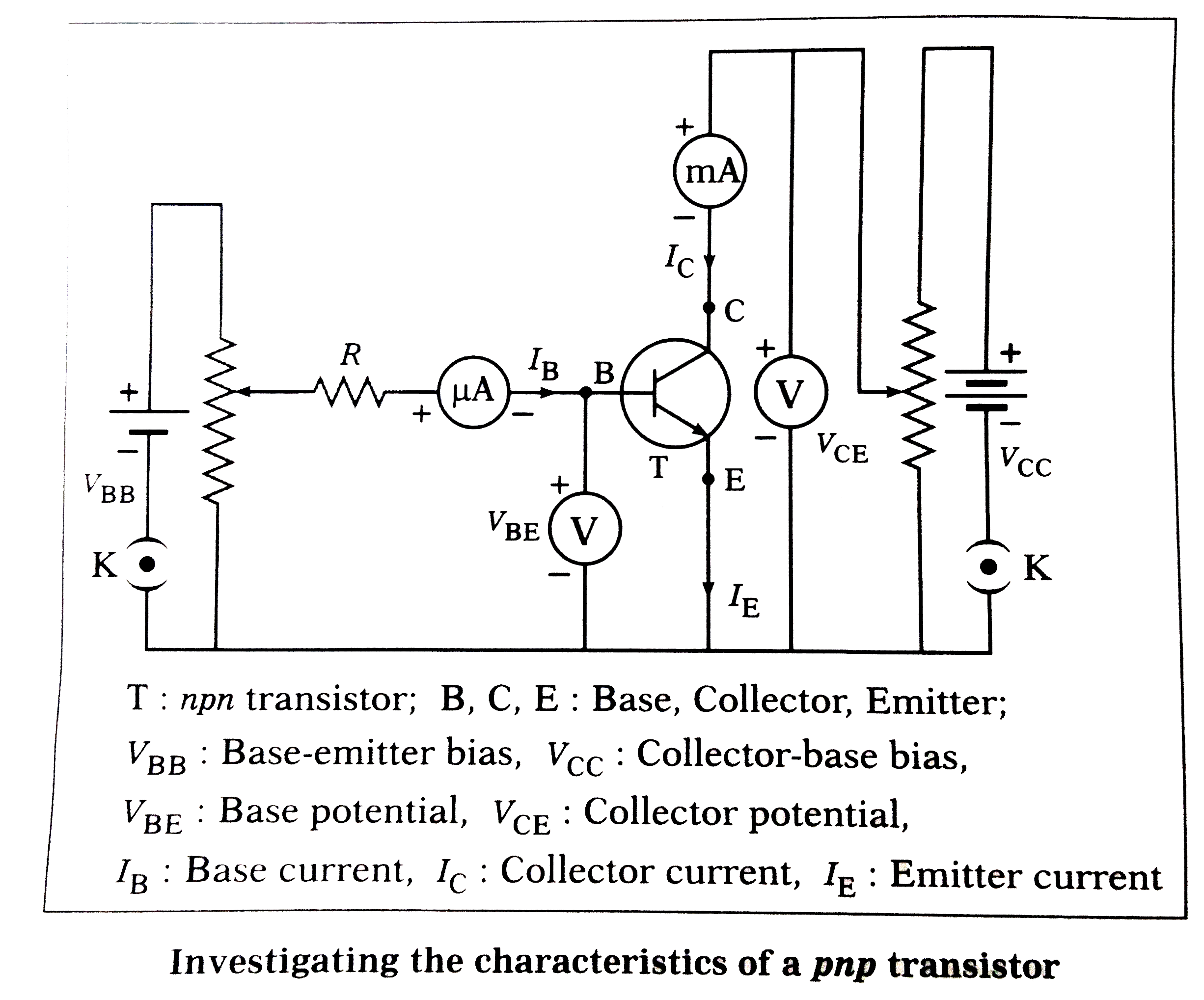
Draw the circuit diagram for studying the characteristics of a transistor in common emitter configuration. Explain briefly and show how input and output characteristics are drawn.

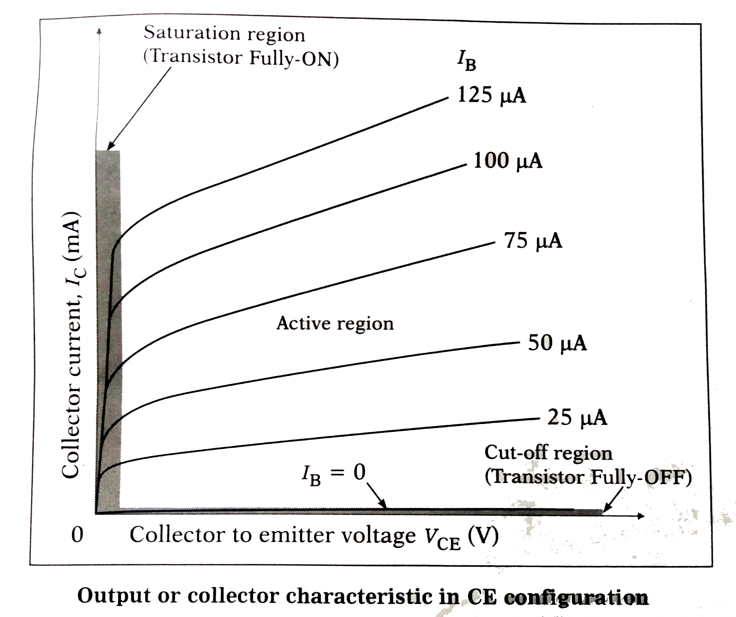
Output or collector characteristics : This is a set of curves of collector current IC against collector-to-emitter voltage VCE for different constant base currents IB, as shown below.

(a) For VBE less than the threshold voltage for the junction, IB=0 and IC=0 i.e., there is no current through the transistor. Both the junctions are reverse biased and the transistor acts like an open switch. Then the transistor is said to be switched Fully-OFF or in the cut-off region or OFF-mode.
(b) The base current is set to a suitable value by varying the base-to-emitter voltage VBE to a value greater than the threshold voltage. Then, the collector-to-emitter voltage VCE is varied and the variation of IC is plotted against VCE. For very small values of VCE, ideally zero, IC is maximum, equal to VCC/RL. Both the junction are forward biased and the transistor acts like a closed switch. The transistor is said to be switched Fully-ON, or in the saturation region or ON-mode.
(c) But for values of VCE above the threshold voltage, IC is constant and VCE has relatively little effect on it. In this region, called as the active region, IC is determined almost entirely by IB. In this region, the common-emitter current gain β is large.
Topper's Solved these Questions
- EXPERIMENTS AND DIAGRAMSBook:NAVNEET PUBLICATION - MAHARASHTRA BOARDChapter:EXPERIMENTS AND DIAGRAMSExercise:ELECTRONS AND PHOTONS
Explore 1 Video
- EXPERIMENTS AND DIAGRAMSBook:NAVNEET PUBLICATION - MAHARASHTRA BOARDChapter:EXPERIMENTS AND DIAGRAMSExercise:ATOMS, MOLECULES AND NUCLEI
Explore 1 Video
- EXPERIMENTS AND DIAGRAMSBook:NAVNEET PUBLICATION - MAHARASHTRA BOARDChapter:EXPERIMENTS AND DIAGRAMSExercise:CURRENT ELECTRICITY
Explore 1 Video
- DISTINGUISH BETWEENBook:NAVNEET PUBLICATION - MAHARASHTRA BOARDChapter:DISTINGUISH BETWEENExercise:Assingment
Explore 3 Videos
- EXPLANATION, CHARACTERISTICS AND PROPERTIES Book:NAVNEET PUBLICATION - MAHARASHTRA BOARDChapter:EXPLANATION, CHARACTERISTICS AND PROPERTIES Exercise:Assignments
Explore 2 Videos
Similar Questions
Draw a circuit diagram to obtain the characteristics of a n-p-n transistor in common base configuration . Give shape of input and output characteristic curves.
View SolutionDraw a circuit diagram to study characteristics of a transistor (pnp or ppn) in common emitter configuration. Draw the sketch of (i) input characterisitics and (ii) output characteristics for this configuration.
View SolutionDraw a circuit diagram to study characteristics of n-p-n transistor in CE configuration. Draw the sketch of input and output characteristics of this configuration . Define current amplification factor ?
View SolutionDefine the dynamic output resistance of a transistor amplifier in common - emitter configuration.
View SolutionDraw the circuit diagram for studying the characteristics of a transistor in common emitter configuration. Explain briefly and show how input and output characteristics are drawn.
View SolutionDraw the circuit diagram for studying the characteristics of a transistor in common emitter configuration. Explain briefly and show how input and output characteristics are drawn.
View SolutionThe typical output characteristics curve for a transistor working in the common-emitter configuration is shown in the figure.

View SolutionWith a neat labelled diagram, explain the actionn of npn transistor in common base configuration
View SolutionDraw circuit diagram for n-p-n transistor to draw input and output characteristics in common base configuration. Draw the input and ouput curves and explain them.
View SolutionWith the help of a labelled circuit diagram, explain how an n-p-n transistor can be used as an amplifier in common-emitter configuration. Explain how the input and output voltages are out of phase by 1800 for a common-emitter transistor amplifier.
View Solution

