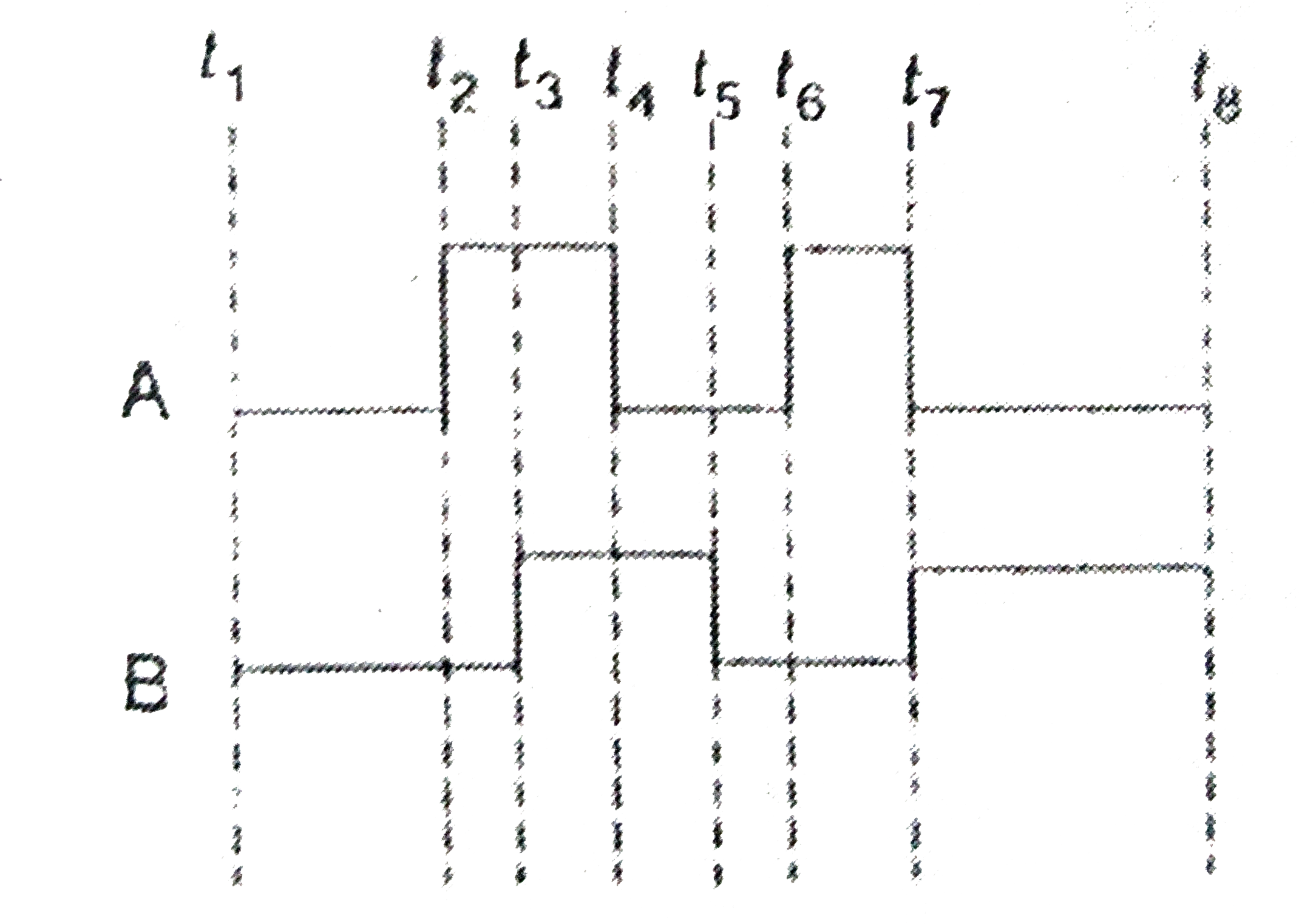
(i) Figure shows the input waveform which is converted by a device .X. into an output wavefrom. Mane the device and explain its working using the proper circuit.
(ii) Draw the forward bias and reverse blas circuit for the basic component of the device and draw the characterstics.
Explain clearly which region of the curve is used in an amplifier.
Step-by-Step Solution
1. Identify the Device:
- The device that converts the input waveform into an output waveform with increased amplitude is an amplifier.
2. Explain the Working of the Amplifier:
- The amplifier works by taking a small input signal and producing a larger output signal.
- A common type of amplifier is the Common Emitter Amplifier.
- In this configuration, the input signal is applied between the base and emitter terminals of a transistor, and the output is taken from the collector terminal.
3. Circuit Diagram:
- Draw the circuit for a common emitter amplifier, including:
- A transistor (NPN or PNP)
- Resistors for biasing (RB for base biasing, RL for load)
- A coupling capacitor (if needed) to block DC components.
- Label the input voltage (Vi) and output voltage (Vo).
4. Operation:
- When a small AC voltage (input signal) is applied to the base-emitter junction, it causes a change in the base current (IB).
- This change in base current leads to a larger change in collector current (IC), due to the transistor's current gain (β).
- The output voltage (Vo) across the load resistor (RL) is then amplified, resulting in a larger output signal.
Part (ii): Forward Bias and Reverse Bias Circuits
1. Forward Bias Circuit:
- Draw the circuit diagram where the transistor is in forward bias:
- Connect the positive terminal of the voltage source to the base and the negative terminal to the emitter.
- Include a resistor (RB) connected to the base for biasing.
- Label the input and output terminals.
2. Reverse Bias Circuit:
- Draw the reverse bias circuit:
- Connect the negative terminal of the voltage source to the base and the positive terminal to the emitter.
- This configuration prevents current flow through the transistor.
- Label the input and output terminals.
3. Characteristics Curve:
- Draw the output characteristics curve for the transistor:
- The x-axis represents the collector-emitter voltage (VCE) and the y-axis represents the collector current (IC).
- Identify the three regions: Cut-off region (no current), Active region (amplification occurs), and Saturation region (maximum current).
4. Region Used in Amplifier:
- Explain that the Active Region of the characteristics curve is used for amplification.
- In this region, the transistor can amplify the input signal, allowing for a proportional increase in output current.
- The device that converts the input waveform into an output waveform with increased amplitude is an amplifier.
- The amplifier works by taking a small input signal and producing a larger output signal.
- A common type of amplifier is the Common Emitter Amplifier.
- In this configuration, the input signal is applied between the base and emitter terminals of a transistor, and the output is taken from the collector terminal.
- Draw the circuit for a common emitter amplifier, including:
- A transistor (NPN or PNP)
- Resistors for biasing (RB for base biasing, RL for load)
- A coupling capacitor (if needed) to block DC components.
- Label the input voltage (Vi) and output voltage (Vo).
- When a small AC voltage (input signal) is applied to the base-emitter junction, it causes a change in the base current (IB).
- This change in base current leads to a larger change in collector current (IC), due to the transistor's current gain (β).
- The output voltage (Vo) across the load resistor (RL) is then amplified, resulting in a larger output signal.
- Draw the circuit diagram where the transistor is in forward bias:
- Connect the positive terminal of the voltage source to the base and the negative terminal to the emitter.
- Include a resistor (RB) connected to the base for biasing.
- Label the input and output terminals.
- Draw the reverse bias circuit:
- Connect the negative terminal of the voltage source to the base and the positive terminal to the emitter.
- This configuration prevents current flow through the transistor.
- Label the input and output terminals.
- Draw the output characteristics curve for the transistor:
- The x-axis represents the collector-emitter voltage (VCE) and the y-axis represents the collector current (IC).
- Identify the three regions: Cut-off region (no current), Active region (amplification occurs), and Saturation region (maximum current).
- Explain that the Active Region of the characteristics curve is used for amplification.
- In this region, the transistor can amplify the input signal, allowing for a proportional increase in output current.
Similar Questions
(a) In the figure given below the input waveform is converted into the output waveform by a device 'X'. Name the device and draw its circuit diagram.

(b) Identify the logic gate represented by the circuit as shown and write its truth table.

View SolutionDraw the output waveform X, using the given inputs A and B for the logic circuit shows below. Also, identify the logic operation performed by this circuit.

View SolutionDraw the output waveformed at X, using the given inputs A and B for the logic circuit shows below. Also, identify the logic operation performed by this circuit.

View SolutionDraw a circuit diagram of a full-wave rectifier. Explain its working principle. Draw the input/output wave forms indicating clearly the function of the two diode used.
View SolutionDraw a circuit diagram of a full-wave rectifier. Explain its working principle. Draw the input/output wave forms indicating clearly the function of the two diode used.
View SolutionDraw the diagram of the circuit arangement used for studying the 'input' and the 'output' characteristics of an n-p-n transistor inits CE configuration. Briefly explain how these two types of characteristics are obtained and draw these characteristics.
(b) 'Define' the terms (i) Input resistance, (ii) Output resistance , (iii) Current amplification factor, for a given transistor.
View Solution(a) Draw the circuit diagram of a full wave rectifier using p-n junction diole. Explain its working and show the output, input waveforms.
(b) Show the output waveforms (Y) for the following inputs A and B of (i) OR gate (ii) NAND gate :

View Solution(i) Draw a circuit diagram to study the input and output characteristics of an n-p-n transistor in its common emitter configuration. Draw the typical input and output characteristics.
(ii) Explain, with the hepl of a circuit diagram, the working of n-p-n transistor as a common emitter amplifier.
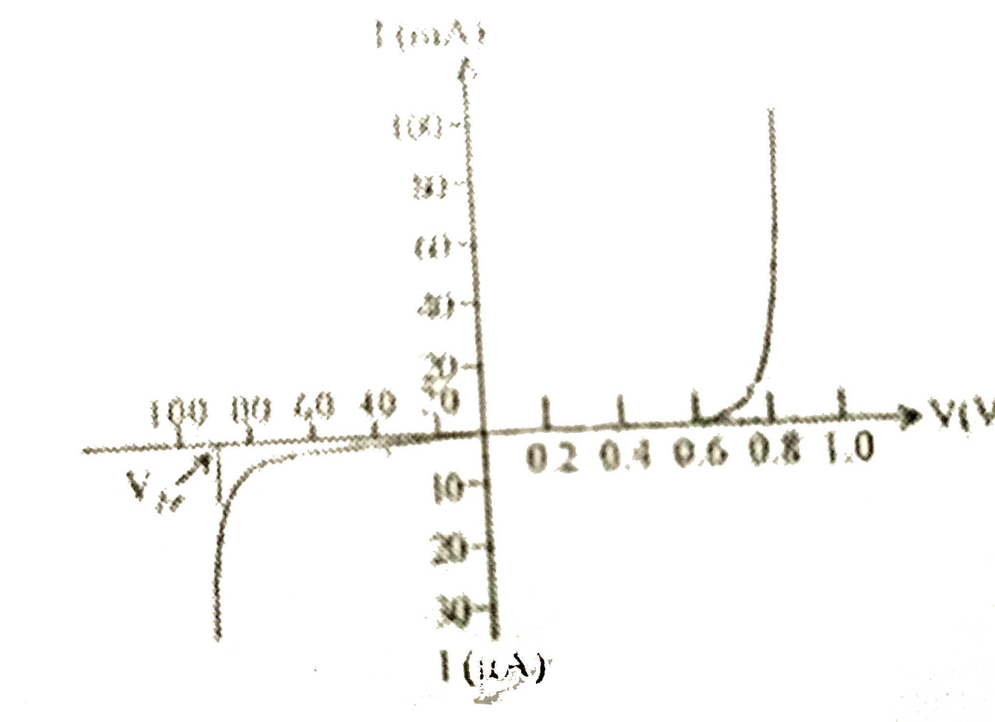
View SolutionThe figure below shows the V-I characteristic of a semiconductor diode.
(i ) Identify the semiconductor diode used.
(ii) Draw the circuit diagram to obtain the given characteristic of this device.
(ii) Briefly explain how this diode can be used as a voltage regulator.

View Solution(i) Write the functions of three segments of a transistor.
(ii) Draw the ciruit diagram or studying the input and output characteristics of n-p-n transisfor in common emitter configuration . Using the circuit explain how input characteristics are obtained .
View Solution