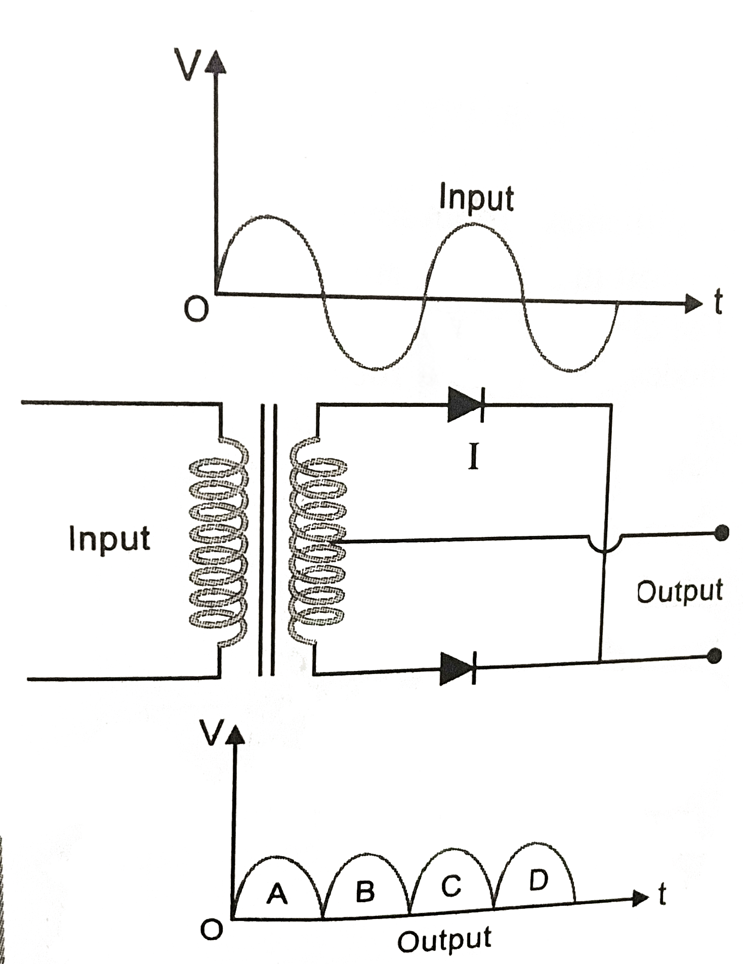
Draw a circuit diagram of a full-wave rectifier. Explain its working principle. Draw the input/output wave forms indicating clearly the function of the two diode used.
Step-by-Step Solution:
Step 1: Draw the Circuit Diagram of a Full-Wave Rectifier
1. Components Required:
- Transformer
- Two Diodes (D1 and D2)
- Load Resistor (R)
2. Circuit Diagram:
- Draw a transformer with primary and secondary coils.
- Connect the AC voltage source to the primary coil.
- Connect the secondary coil to two diodes (D1 and D2) in such a way that they are oriented in opposite directions.
- Connect the output of the diodes to a load resistor (R).
The circuit diagram will look like this:
ACSource||±−−⊢−+|||||||()|Tranormer|||±−−⊢−+|⊢−−→D1−−−−→+−−−−→Load(R)−−−−→||∣||∣⊢−−→D2−−−−→−
Step 2: Explain the Working Principle
1. First Half Cycle:
- During the positive half cycle of the AC input, point A becomes positive and point B becomes negative.
- Diode D1 is forward biased (conducting), allowing current to flow through the load.
- Diode D2 is reverse biased (non-conducting), so no current flows through it.
2. Second Half Cycle:
- During the negative half cycle, point A becomes negative and point B becomes positive.
- Diode D1 is now reverse biased (non-conducting), so no current flows through it.
- Diode D2 is forward biased (conducting), allowing current to flow through the load.
3. Result:
- The output current flows through the load during both half cycles, resulting in a pulsating DC output.
Step 3: Draw Input/Output Waveforms
1. Input Waveform:
- The input waveform is a sinusoidal AC voltage, which oscillates between positive and negative values.
2. Output Waveform:
- The output waveform is a series of positive pulses. During the positive half cycle, the output follows the input, and during the negative half cycle, the output is also positive due to the conduction of D2.
The waveforms can be represented as follows:
InputVo<a≥(V∈)∣∣∣
∣
∣
∣
∣
∣
∣
∣
∣∣/ ∣∣/ ⊢−−−−−−−−−−−−/−−−−−−−∣∣/ ∣∣∣/ ⌊__/____⊢−−−−−−−−−−−−−−−−−−−−−−−−−−−−−−−−−−→Time<p><p>OutputVo<a≥(Vout)∣∣∣∣∣
∣
∣
∣
∣
∣
∣
∣
∣∣ /∣∣/ ⊢−−−−−−−−−−−−/−−−−−−−∣∣ /∣ /⎢⎢
⎢
⎢
⎢
⎢
⎢
⎢
⎢
⎢
⎢
⎢
⎢
⎢
⎢
⎢
⎢
⎢
⎢
⎢
⎢
⎢
⎢
⎢
⎢
⎢
⎢
⎢
⎢
⎢
⎢
⎢
⎢
⎢
⎢
⎢
⎢
⎢
⎢
⎢
⎢
⎢
⎢
⎢
⎢
⎢
⎢
⎢
⎢
⎢
⎢
⎢
⎢
⎢
⎢
⎢
⎢
⎢
⎢
⎢
⎢
⎢
⎢
⎢
⎢
⎢
⎢
⎢
⎢
⎢⎣__/____⊢−−−−−−−−−−−−−−−−−−−−−−−−−−−−−−−−−−→Time
- In the output waveform, both halves of the input waveform are represented as positive pulses.
- Transformer
- Two Diodes (D1 and D2)
- Load Resistor (R)
2. Circuit Diagram:
- Draw a transformer with primary and secondary coils.
- Connect the AC voltage source to the primary coil.
- Connect the secondary coil to two diodes (D1 and D2) in such a way that they are oriented in opposite directions.
- Connect the output of the diodes to a load resistor (R).
- During the positive half cycle of the AC input, point A becomes positive and point B becomes negative.
- Diode D1 is forward biased (conducting), allowing current to flow through the load.
- Diode D2 is reverse biased (non-conducting), so no current flows through it.
- During the negative half cycle, point A becomes negative and point B becomes positive.
- Diode D1 is now reverse biased (non-conducting), so no current flows through it.
- Diode D2 is forward biased (conducting), allowing current to flow through the load.
- The output current flows through the load during both half cycles, resulting in a pulsating DC output.
- The input waveform is a sinusoidal AC voltage, which oscillates between positive and negative values.
- The output waveform is a series of positive pulses. During the positive half cycle, the output follows the input, and during the negative half cycle, the output is also positive due to the conduction of D2.
∣
∣
∣
∣
∣
∣
∣
∣∣/ ∣∣/ ⊢−−−−−−−−−−−−/−−−−−−−∣∣/ ∣∣∣/ ⌊__/____⊢−−−−−−−−−−−−−−−−−−−−−−−−−−−−−−−−−−→Time<p><p>OutputVo<a≥(Vout)∣∣∣∣∣
∣
∣
∣
∣
∣
∣
∣
∣∣ /∣∣/ ⊢−−−−−−−−−−−−/−−−−−−−∣∣ /∣ /⎢⎢
⎢
⎢
⎢
⎢
⎢
⎢
⎢
⎢
⎢
⎢
⎢
⎢
⎢
⎢
⎢
⎢
⎢
⎢
⎢
⎢
⎢
⎢
⎢
⎢
⎢
⎢
⎢
⎢
⎢
⎢
⎢
⎢
⎢
⎢
⎢
⎢
⎢
⎢
⎢
⎢
⎢
⎢
⎢
⎢
⎢
⎢
⎢
⎢
⎢
⎢
⎢
⎢
⎢
⎢
⎢
⎢
⎢
⎢
⎢
⎢
⎢
⎢
⎢
⎢
⎢
⎢
⎢
⎢⎣__/____⊢−−−−−−−−−−−−−−−−−−−−−−−−−−−−−−−−−−→Time
Topper's Solved these Questions
- XII BOARDSBook:XII BOARD PREVIOUS YEAR PAPER ENGLISHChapter:XII BOARDSExercise:PHYSICS (Theory) DELHI BOARD -2016 [SET -I][COMPTT.]
Explore 11 Videos
- XII BOARDSBook:XII BOARD PREVIOUS YEAR PAPER ENGLISHChapter:XII BOARDSExercise:C.B.S.E.CLASS-XII PHYSICS (THEORY) [SET-I] (SECTION-A)
Explore 5 Videos
- XII BOARDSBook:XII BOARD PREVIOUS YEAR PAPER ENGLISHChapter:XII BOARDSExercise:SECTION-B
Explore 52 Videos
- SAMPLE PAPER 2019Book:XII BOARD PREVIOUS YEAR PAPER ENGLISHChapter:SAMPLE PAPER 2019Exercise:SECTION D
Explore 6 Videos
Similar Questions
Draw the circuit diagram of a half - wave rectifier using a p-n junction diode.
View SolutionDraw a neatly labelled circuit diagram of a full wave rectifier using two junction diodes.
View SolutionWhat is the output form of full-wave rectifier ?
View SolutionDraw a simple diagram of a hydraulic jack and explain its working.
View SolutionDraw a labelled circuit diagram of a half wave rectifier and give its output waveform.
View Solution(a) Draw the circuit diagram of a full wave rectifier using p-n junction diole. Explain its working and show the output, input waveforms.
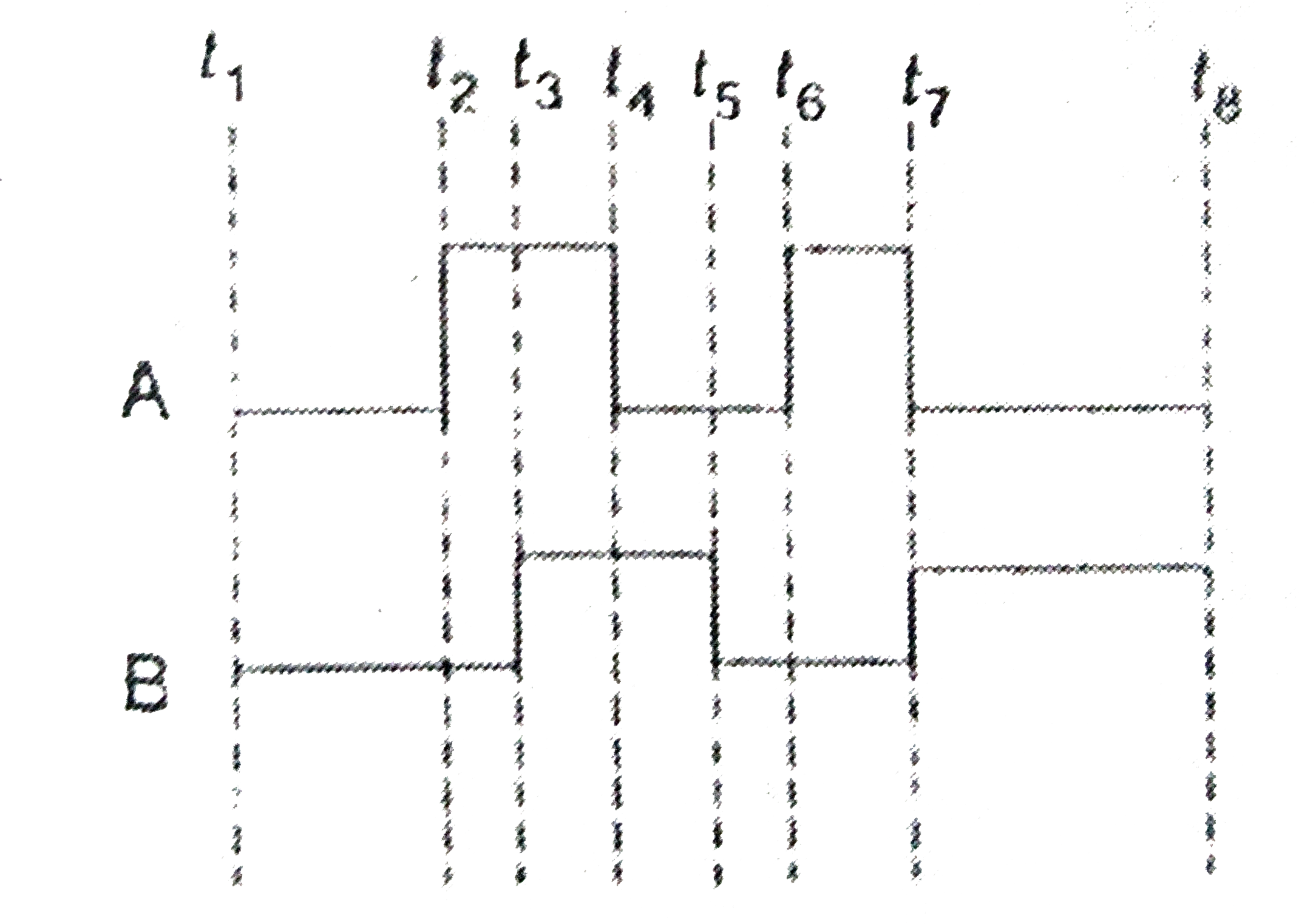
(b) Show the output waveforms (Y) for the following inputs A and B of (i) OR gate (ii) NAND gate :

View SolutionDraw a schematic diagram of a cyclotron. Explain its underlying principle and working, stating clearly the function of the electric and magnetic fields applied on a charged particle.
Deduce an expression for the period of revolution and show that it does not depend on the speed of the charged particle.
View SolutionDraw a schematic diagram of a step-up transformer . Explain its working principle . Deduce the expression for the secondary to primary voltage in terms of the number of turns in the two coils . In an ideal transformer , how is this ratio related to the currents in the two coils ?
View SolutionA full wave rectifier circuit along with the input and output are shown in Fig. the concentrations from the diode I is (are)

View SolutionA full wave rectifier circuit along with the input and output are shown in the figure. The contribution from the diode D2 is (are)
View Solution

