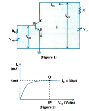
Consider the circuit arrangement shown in figure (1) for studying input and output characteristics of n-p-n transistor in CE configuration.
Select the values of RB and RC for a transistor whose VBE=0.7V, so that the transistor is operating at point Q as shown in the characteristics shown in figure (2). Given that the input impedance of the transistor is very small and VCC=VBB=16V, also find the voltage gain and power gain of circuit making appropriate assumptions. Solution in Gujrati
Graph in figure-2 is for IB=30μA. For point Q on it, IC=4mA=4×10⁻³AandVCE=8V
For output part of above figure,
VCC=ICRC+VCE
∴16=(4×10⁻³)RC+8
∴RC=84×10−3=2×10³Ω=2kΩ
For input part of above figure-1,
VBB=IBRB+VBE
∴16=(30×10−6)RB+0.7
∴RB=15.330×10−6=5.1×10⁵Ω=510×103Ω
=510kΩ
Voltage gained,
AV=βRCRB=(ICIB)(RCRB)
∴Av=(4×10−330×10−6)(2×103510×103)
∴AV=0.52
Power gained,
AP=AVAi=AVβ=AV(ICIB)
∴AP=0.52×4×10−330×10−6
∴AP=69.33
Topper's Solved these Questions
- SEMICONDUCTOR ELECTRONICS : MATERIALS, DEVICES AND SIMPLE CIRCUITS BOOK - KUMAR PRAKASHANCHAPTER - SEMICONDUCTOR ELECTRONICS : MATERIALS, DEVICES AND SIMPLE CIRCUITS EXERCISE - Section-D : Multiple Choice Questions (MCQs) (MCQs From .DARPAN. Based On Textbook)
116 Videos
- SEMICONDUCTOR ELECTRONICS : MATERIALS, DEVICES AND SIMPLE CIRCUITS BOOK - KUMAR PRAKASHANCHAPTER - SEMICONDUCTOR ELECTRONICS : MATERIALS, DEVICES AND SIMPLE CIRCUITS EXERCISE - Section-D : Multiple Choice Questions (MCQs) (MCQs asked in Competitive Exams)
129 Videos
- SEMICONDUCTOR ELECTRONICS : MATERIALS, DEVICES AND SIMPLE CIRCUITS BOOK - KUMAR PRAKASHANCHAPTER - SEMICONDUCTOR ELECTRONICS : MATERIALS, DEVICES AND SIMPLE CIRCUITS EXERCISE - Section-C: NCERT Exemplar Solution (Short Answer Type Questions)
8 Videos
- SAMPLE QUESTION PAPER BOOK - KUMAR PRAKASHANCHAPTER - SAMPLE QUESTION PAPER EXERCISE - PART-B SECTION-C
5 Videos
- WAVE OPTICSBOOK - KUMAR PRAKASHANCHAPTER - WAVE OPTICSEXERCISE - SECTION-D (MULTIPLCE CHOICE QUESTIONS (MCQS)) (MCQS FROM DARPAN BASED ON TEXTBOOK)
239 Videos
Similar Questions
Which of the following is not a conductor of electricity?
View SolutionAt absolute zero temperature Si acts as ……..
View Solution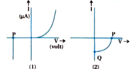
(i) Name the type of a diode whose characteristics are shown in figure (1) and figure (2).
(ii) What does the point P in figure (1) represent?
(iii) What does the points P and Q in figure (2) represent?
View SolutionTwo charges –q and +q are located at points (0, 0, –a) and (0, 0, a), respectively.
(a) What is the electrostatic potential at the points (0, 0, z) and (x, y, 0) ?
(b) Obtain the dependence of potential on the distance r of a point from the origin when r/a>>1 .
(c) How much work is done in moving a small test charge from the point (5,0,0) to (–7,0,0) along the x-axis? Does the answer change if the path of the test charge between the same points is not along the x-axis?
View SolutionAccording to particle theory of light what is the velocity of light in a dense medium, compared to that in rare medium ?
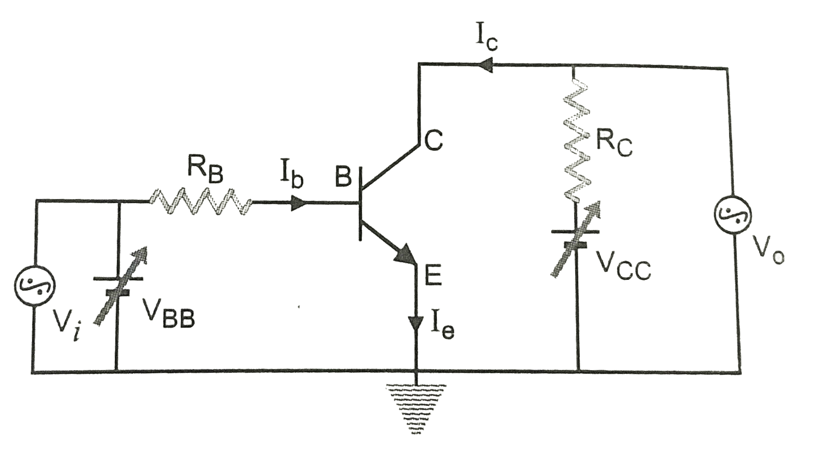
View SolutionIn common emitter transistor as shown in Fig., the VBB supply can be varied from 0 V to 5.0V. The Si. Transistor has βac=250 and RB=100kΩ,Rc=1kΩ,VCC=5.0V. Assume that when the transistor is saturated, VCE=0V and VBE=0.8V. Calculate the minimum base current, for which the transistor will reach saturation. Hance, determine Vi when the transistor is 'switched on' find ranges of Vi for which the transistor is switched off and switched on.
View SolutionConsider the circuit arrangnent shown in Fig. for studying input and output characteristics of npn transistor in CE configuration.
Select the values of R and R for a transistor whose VBE=0.7V, so that the transistor is operating at point Q as shown in the characteristics shown in Fig.
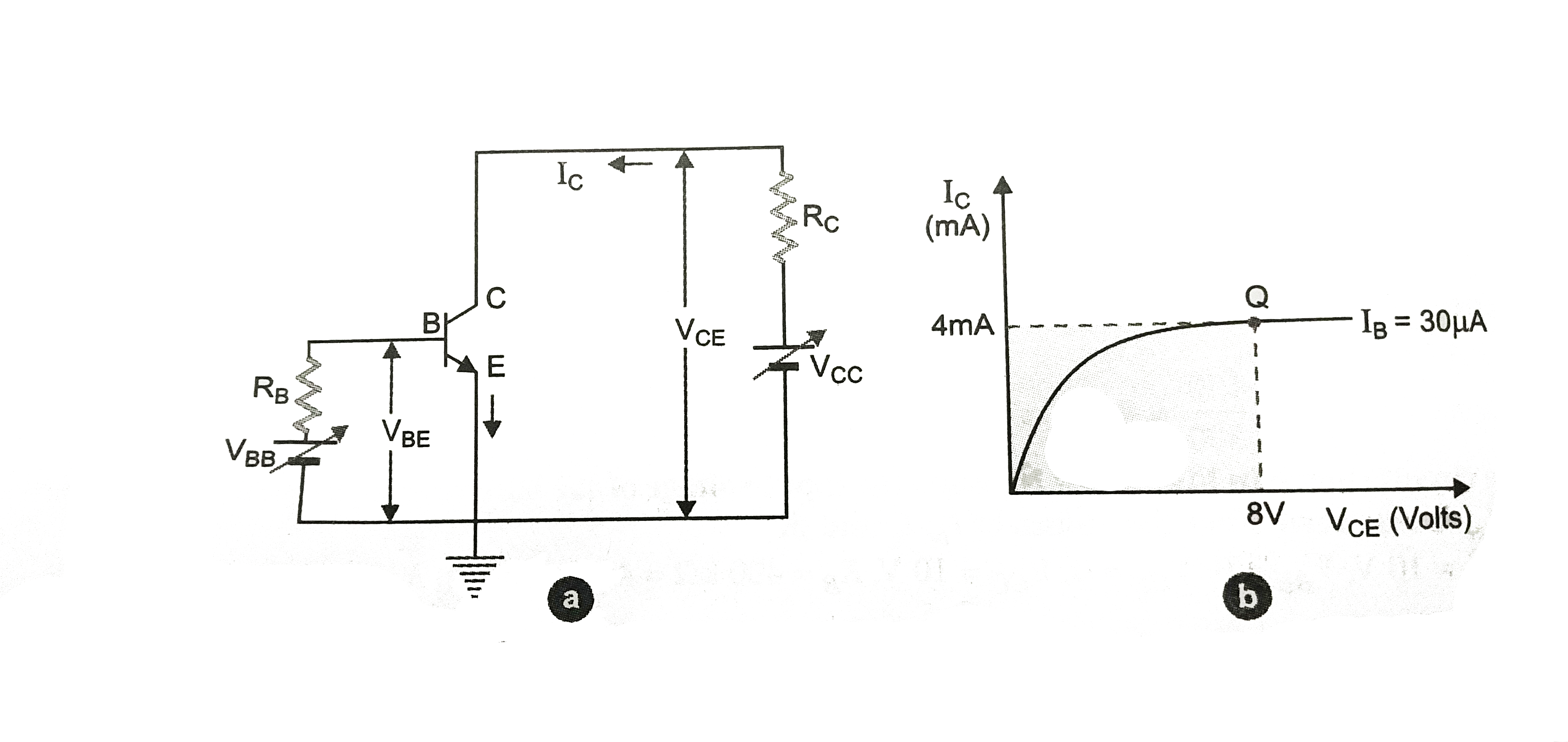 Given that the input impedance of the transistor is very small and VCC=VBB=16V, also find the voltage gain and power gain of circuit making appropriate assumptions.
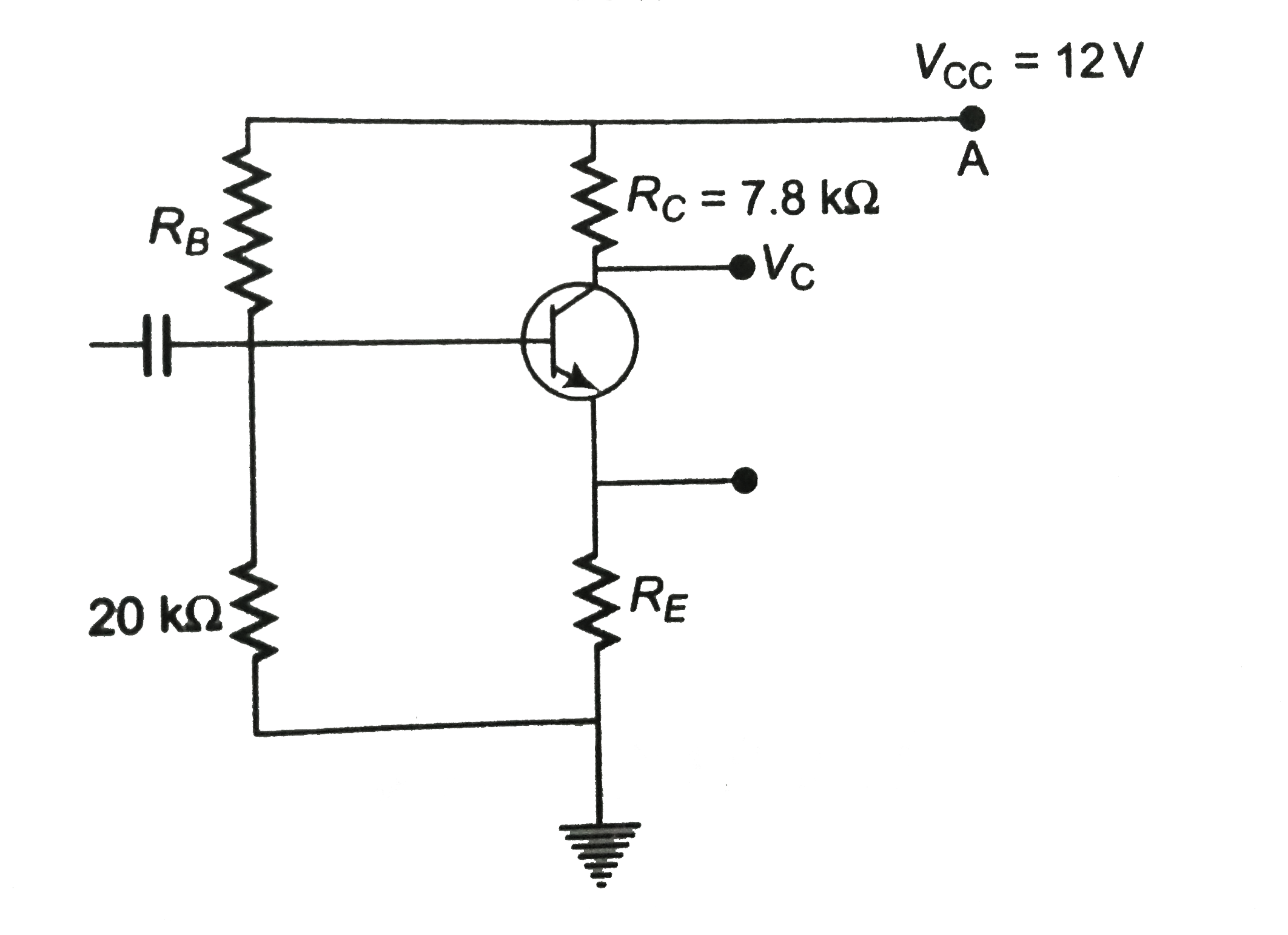
View SolutionFor the transistor circuit shown in figure , evaluate VE,RBandRE. Given IC=1mA,
VCE=3V,VBE=0.5V,VC=12Vandβ=1000
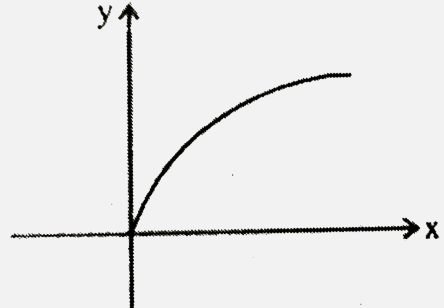
View SolutionWhich is correct for the graph ?
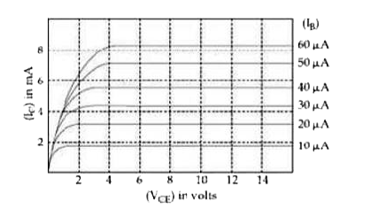
View SolutionOutput characteristic of n-p-n transistor in CE configuration is shown. From the characteristic curve determine the current gain at V_(CE)=1V -
View SolutionShow the circuit arrangement for studying the input and output characteristics of a n-p-n transistor in CE configuration.
View SolutionThe output characteristics of a transistor is shown in the figure. When VCE is 10 V and IC=4.0mA, then value of βac is _________
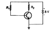
View SolutionAn n-p-n transistor is connected in common - emitter configuration as shown in VBE=0.6V,VCE=3 and common - emitter current amplification factor is 50, then the values of R1 and R2 are respectively.
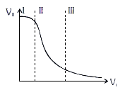
View Solutionकिसी भी आधार बायसित ट्राँजिस्टर के लिये CE विन्यास में अन्तरण अभिलक्षण [निर्गत वोल्टता (V0) तथा निवेश वोल्टता (Vi) के बीच ] आरेख में दर्शाया गया है। ट्रांजिस्टर का स्विच के रूप में उपयोग करने के लिये, इस का उपयोग किया जात है।
View SolutionConsider the circuit arrangnent shown in Fig. for studying input and output characteristics of npn transistor in CE configuration. Select the values of R_ and R_ for a transistor whose V_(BE)=0.7V , so that the transistor is operating at point Q as shown in the characteristics shown in Fig. Given that the input impedance of the transistor is very small and V_(C C)=V_(BB)=16V , also find the voltage gain and power gain of circuit making appropriate assumptions.
View Solution

