Write the definition of valence band and conduction band. Solution in Gujrati
Some solids have a crystalline structure means there is a systematic arrangement of atoms or molecules in it.
When atoms are arranged close to each other the atom gets interact with neighbouring atoms and other atoms as a result energy of electrons of atoms are changed.
The energy level of inner shells electrons are not affected, but the energy levels of the outer shells electrons (valence electron) are changed, since these electrons are shared, by more than one atom in the crystal.
The electrons of the atoms in the crystal has closely spaced different energy levels instead of widely separated energy level of electrons of isolated atom. Such a band of close energy levels is called energy band.
The valence electrons (in last counter orbit) are called as valence electrons in incomplete orbit. The energy band which includes the energy levels of the valence electrons is called the valence band.
The energy band above the valence band is called the conduction band.
Usually a valence band has a valence electron while no electron in conduction band.
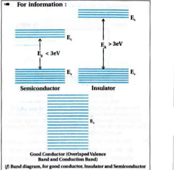
There is some gap between the conduction band and the valence band. The energy difference of this empty space is called band gap energy (Eg).
When the minimum energy level of the conduction band is lower than the higher energy level of the valence band, the electrons in the valence band can easily move to the conduction band. This happens in metals (conductors).
If there is some gap between the conduction band and the valence band, electrons in the valence band all remain bound and no free electrons are available in the conduction band. This makes the material an insulator.
If the distance between the conduction band and the valence band is relatively small and if some of the electrons in the valence band get external energy crosses band gap energy and goes into the conduction band then there is a possibility of flow in conduction band as well as the electron going from the valence band in the conduction band there is a possibility of conduction due to empty spaces in the valence band. This is only possible in the semiconductor.

Topper's Solved these Questions
- SEMICONDUCTOR ELECTRONICS : MATERIALS, DEVICES AND SIMPLE CIRCUITS BOOK - KUMAR PRAKASHANCHAPTER - SEMICONDUCTOR ELECTRONICS : MATERIALS, DEVICES AND SIMPLE CIRCUITS EXERCISE - Section-B : Numericals (Numerical From Textual illustrations)
16 Videos
- SEMICONDUCTOR ELECTRONICS : MATERIALS, DEVICES AND SIMPLE CIRCUITS BOOK - KUMAR PRAKASHANCHAPTER - SEMICONDUCTOR ELECTRONICS : MATERIALS, DEVICES AND SIMPLE CIRCUITS EXERCISE - Section-B : Numericals (Numerical From Textual Exercise)
15 Videos
- SEMICONDUCTOR ELECTRONICS : MATERIALS, DEVICES AND SIMPLE CIRCUITS BOOK - KUMAR PRAKASHANCHAPTER - SEMICONDUCTOR ELECTRONICS : MATERIALS, DEVICES AND SIMPLE CIRCUITS EXERCISE - Section-D : Multiple Choice Questions (MCQs) (MCQs asked in Competitive Exams)
129 Videos
- SAMPLE QUESTION PAPER BOOK - KUMAR PRAKASHANCHAPTER - SAMPLE QUESTION PAPER EXERCISE - PART-B SECTION-C
5 Videos
- WAVE OPTICSBOOK - KUMAR PRAKASHANCHAPTER - WAVE OPTICSEXERCISE - SECTION-D (MULTIPLCE CHOICE QUESTIONS (MCQS)) (MCQS FROM DARPAN BASED ON TEXTBOOK)
239 Videos
Similar Questions
C, Si and Ge have same lattice structure. Why is C insulator while Si and Ge intrinsic semiconductors?
View SolutionIn an n type silicon, which of the following statements is true:
View SolutionAt absolute zero temperature Si acts as ……..
View SolutionTwo charges –q and +q are located at points (0, 0, –a) and (0, 0, a), respectively.
(a) What is the electrostatic potential at the points (0, 0, z) and (x, y, 0) ?
(b) Obtain the dependence of potential on the distance r of a point from the origin when r/a>>1 .
(c) How much work is done in moving a small test charge from the point (5,0,0) to (–7,0,0) along the x-axis? Does the answer change if the path of the test charge between the same points is not along the x-axis?
View SolutionAccording to particle theory of light what is the velocity of light in a dense medium, compared to that in rare medium ?
View SolutionThe conduction band and valency band of a good conductors are
View SolutionIn insulators (CB is conduction band and VB is valence band )
View Solutionसंयोजकता बैण्ड, चालन बैण्ड और ऊर्जा अन्तराल क्या है ?
View Solutionकुचालक पदार्थ में संयोजकता पट्टी (valence band ) तथा चालकता पट्टी (conduction band ) के बीच
View SolutionThe gap between the conduction band and valence band is largest in
View SolutionThe energy band gap between valence band and conduction band is maximum in
View SolutionWrite the definition of valence band and conduction band.
View Solutionwhich of the following statements are true about metals ?
(a) Valence band overlaps with conduction band
(b)the gap between valence band and conduction band is negligible
(c) the gap[ between valence band and conduction band cannot be determined
(d) Valence band may remain partially filled
View SolutionThe conduction band and valence band in a good conductor
View Solutionin insulatore (C.B. is conduction band and V.B. is a valence band)
View SolutionCompare valence band and conduction band.
View Solution
