Describe the function of a transistor as an amplifier with the neat circuit diagram.Sketch the input and output wave form.Solution in Tamil
Transistor as an amplifier:
A transistor operating in the active region has the capability to amplify weak signals. Amplification is the process of increasing the signal strength (increase in the amplitude). If a large amplification is required, the transistors are cascaded with coupling elements like resistors, capacitors, and transformers which is called as multistage amplifiers.
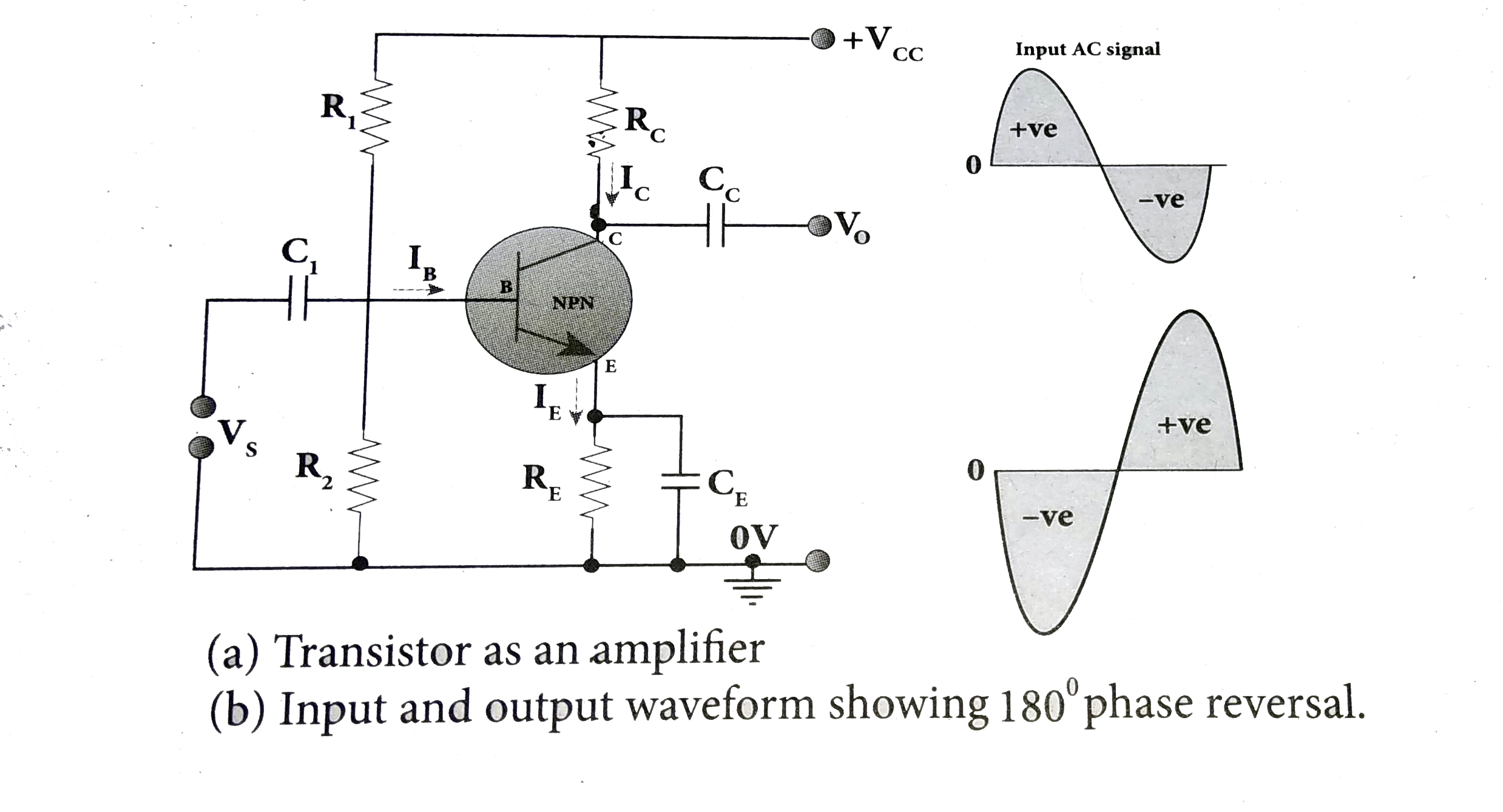
Here, the amplification of an electrical signal is explained with a single stage transistor amplifier as shown in figure (a). Single stage indicates that the circuit consists of one transistor with the allied components. An NPN transistor is connected in the common emitter configuration.

To start with, the point or the operating point of the transistor is fixed so as to get the maximum signal swing at the output (neither towards saturation point nor towards cut-off). A load resistance, RC, is connected in series with the collector circuit to measure the output voltage. The capacitor C1, allows only the ac signal to pass through. The emitter bypass capacitor CE provides a low reactance path to the amplified ac signal. The coupling capacitor C, is used to couple one stage of the amplifier with the next stage while constructing multistage amplifiers. V is the sinusoidal input signal source applied across the base-emitter. The output is taken across the collector-emitter.
Collector current, IC=βIB[∵β=ICIB]
Applying Kirchhoff.s voltage law in the output loop, the collector-emitter voltage is given by VCE=VC−ICRC
Working of the amplifier:
. During the positive half cycle
Input signal (Vs) increases the forward voltage across the emitter-base. As a result, the base current (IB) increases. Consequently, the collector current (IC) increases B times. This increases the voltage drop across R, which in turn decreases the collector-emitter voltage (VCE). Therefore, the input signal in the positive direction produces an amplified signal in the negative direction at the output. Hence, the output signal is reversed by 180° as shown in figure (b).
• During the negative half cycle
Input signal (Vs) decreases the forward voltage across the emitter-base. As a res base current (IB). decreases and in turn increases the collector current (IC). The increase in collector current (1) decreases the potential drop across R and increases the collector-emitter voltage (VCE). Thus, the input signal in the negative direction produce an amplified signal in the positive direction at the output. Therefore, 180∘ phase reversal is observed during the negative half cycle of the input signal.
Topper's Solved these Questions
- SAMPLE PAPER-05 ( SOLVED ) BOOK - FULL MARKSCHAPTER - SAMPLE PAPER-05 ( SOLVED ) EXERCISE - PART-III
9 Videos
- SAMPLE PAPER 9BOOK - FULL MARKSCHAPTER - SAMPLE PAPER 9EXERCISE - PART-IV
10 Videos
- SAMPLE PAPER-07 (SOLVED )BOOK - FULL MARKSCHAPTER - SAMPLE PAPER-07 (SOLVED )EXERCISE - (PART - IV)(Answer all the questions.)
10 Videos
Similar Questions
Give the relation between electric field and electric potential .
View SolutionHow do we determine the electric field due to a continuous charge distribution ? Explain. Electric field due to continous charge distribution
View SolutionCalculate the electric field due to a dipole on its equatorial plane. (OR) Electric field due to an electric dipole at a point on the equatorial plane
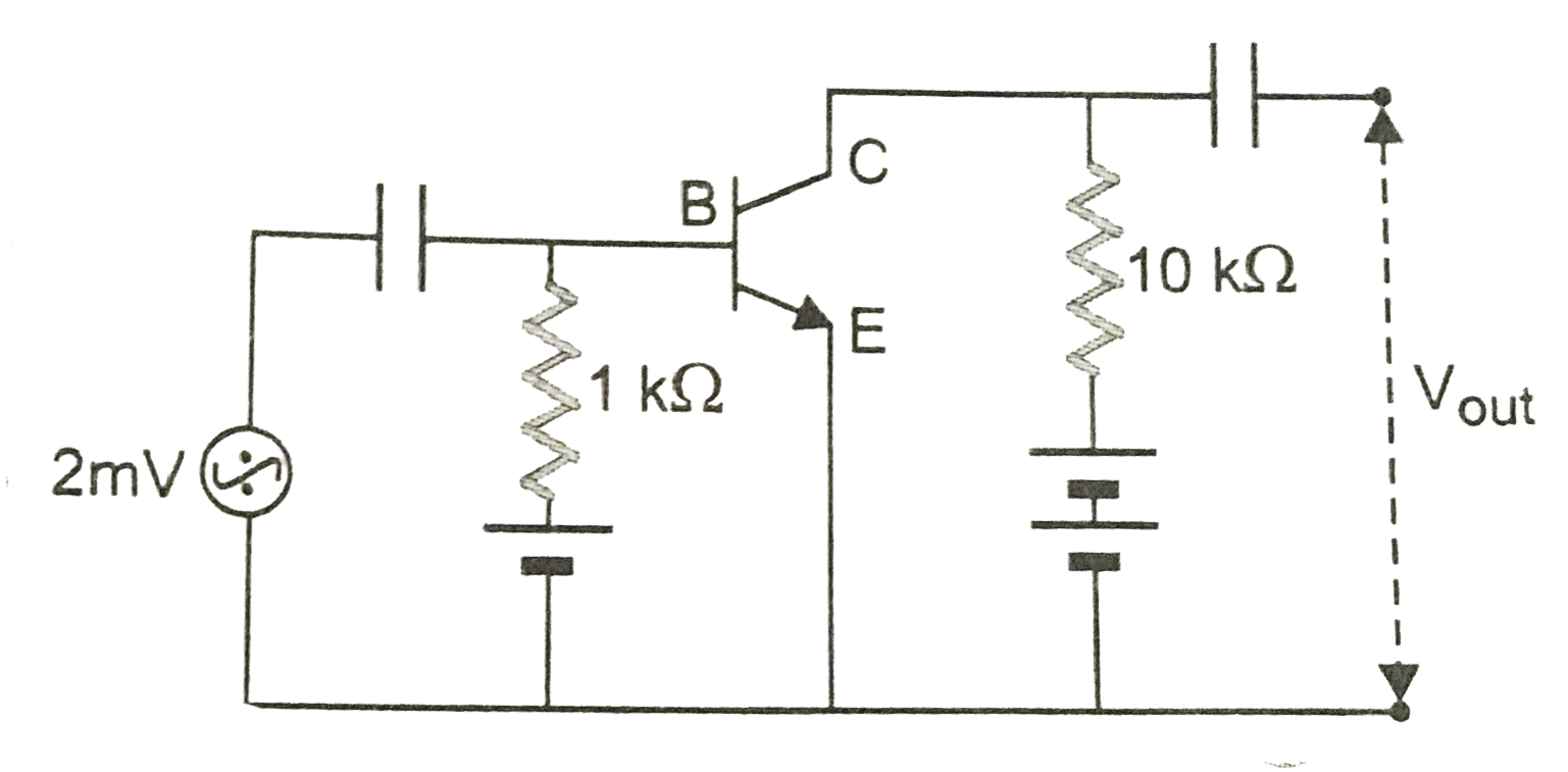
View SolutionIn the common emitter amplifier circuit, Fig. an npn transistor with output voltage of the amplifier as 1 V, the current gain of transistor amplifier is :

View SolutionIn common emitter transistor amplifier circuit, the input signal voltage and the output collector voltage are ..............phase.
View SolutionIn a common emitter amplifier circuit using an n-p-n transistor, the phase difference between the input and the output voltages will be:-
View Solutionn - p - n ट्रांजिस्टर से बनाये हुए एक उभयनिष्ठ-उत्सर्जक प्रवर्धक परिपथ में निवेशित तथा निर्गत विभवों के बीच कलान्तर का मान होगा :
View SolutionDraw a circuit diagram of a CE amplifier by using n-p-n transistor and show input and output voltages graphically.
View SolutionIn a common-emitter amplifier circuit using an n-p-n transistor the phase differene between the input and the output voltages will be
View Solutionट्रान्जिस्टर के उभयनिष्ठ उत्सर्जक प्रवर्धक परिपथ के लिए निवेशी एवं निर्गत सिग्नल के मध्य कलान्तर होता है :
View SolutionDescribe the function of a transistor as an amplifier with the neat circuit diagram. Sketch the input and output wave form.
View SolutionDescribe the function of a transistor as an amplifier with the neat circuit diagram. Sketch the input and output wave form.
View SolutionDescribe the function of a transistor as an amplifier with the neat circuit diagram. Sketch the input and output wave form.
View SolutionIn a common emitter amplifier circuit using a n-p-n transistor, the phase difference between the input and the output voltages will be ……..
View SolutionDraw the labelled circuit diagram of a common-emitter transistor amplifier : Explain clearly how the input and output signals are in opposite phase.
View Solution
