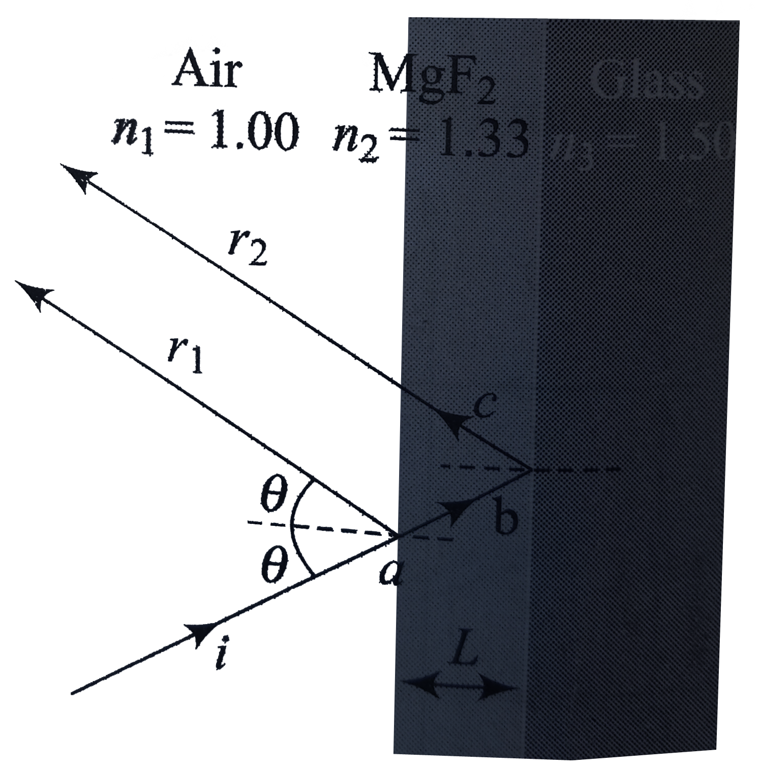
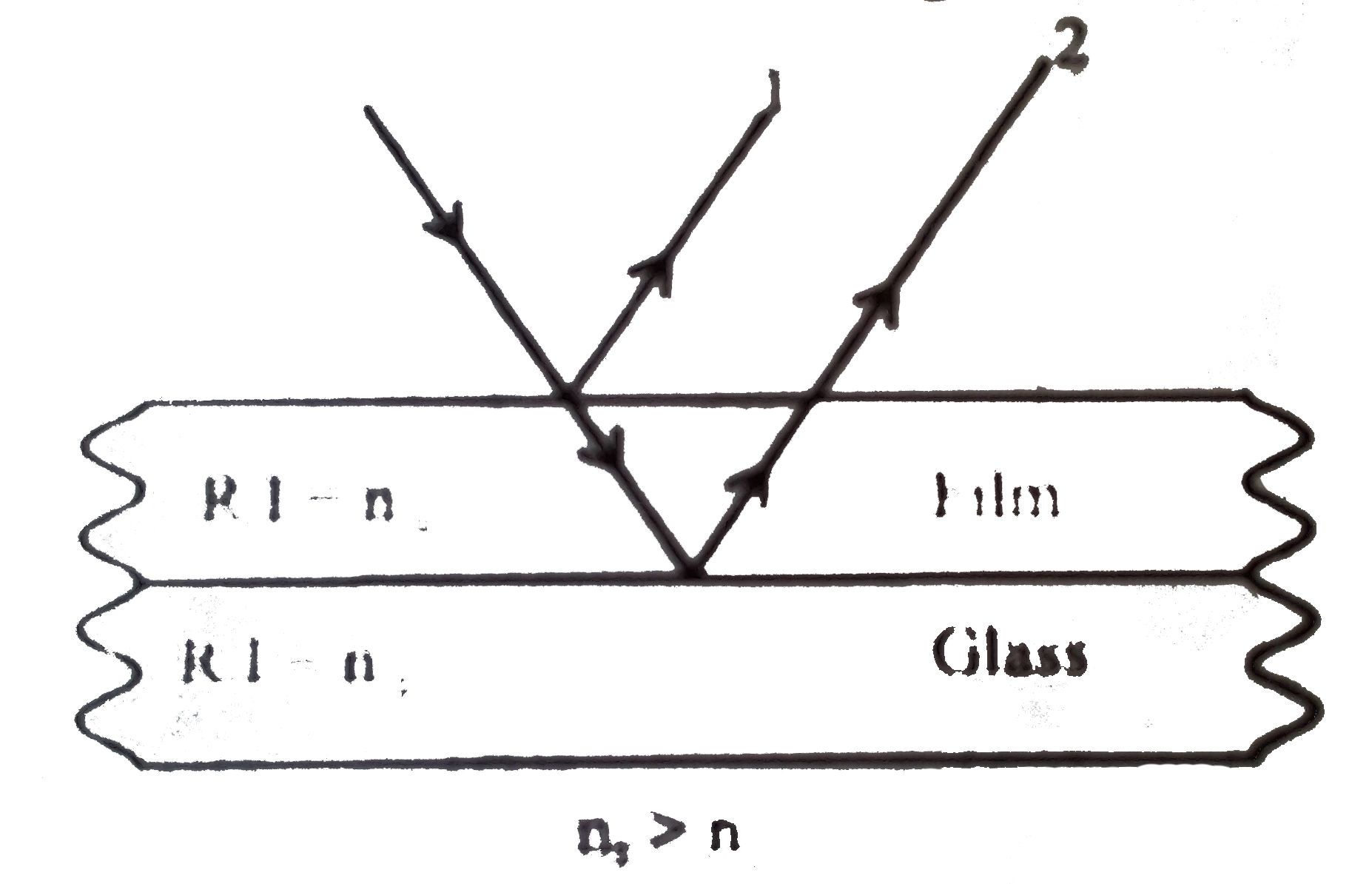
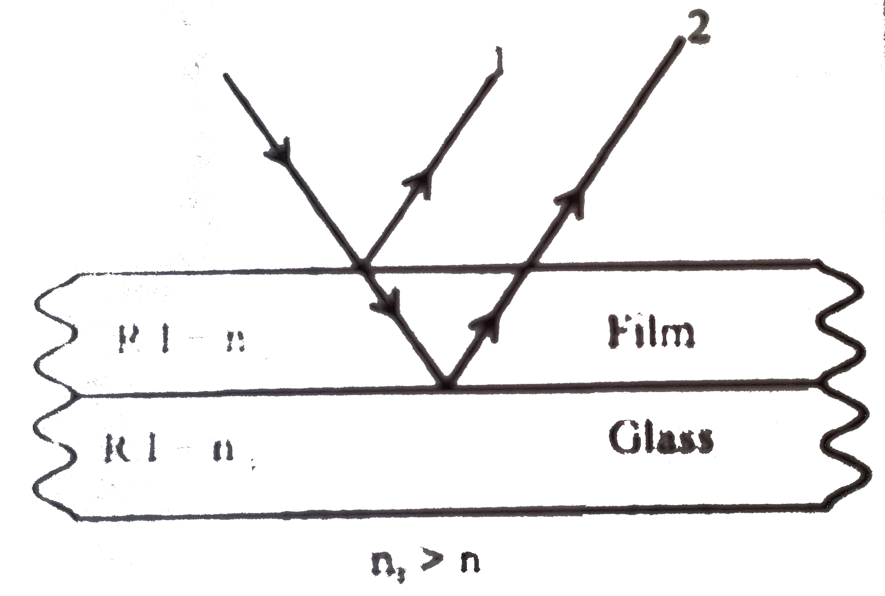
A thin film of a specific meterial can be used to decrease the intensity of reflected light. There is destrucive inteference of wave reflected from upper and lower surface of the film. These films are called non-reflecting or anti-reflecting coatings. The process of coating the lens or surface with non-reflecting film is called blooming as shown in figure The refracting index of coating (n1) is less than that of the glass (n2).

4. If a light of wavelength λ is incident normally and the thickness of film is t, then optical path difference between waves reflected from upper and lower surface of the film is
2n1t
2n1t−λ2
2n1t+λ2
None
The correct Answer is:A
Step by step video, text & image solution for A thin film of a specific meterial can be used to decrease the intensity of reflected light. There is destrucive inteference of wave reflected from upper and lower surface of the film. These films are called non-reflecting or anti-reflecting coatings. The process of coating the lens or surface with non-reflecting film is called blooming as shown in figure The refracting index of coating (n_(1)) is less than that of the glass (n_(2)). 4. If a light of wavelength lambda is incident normally and the thickness of film is t, then optical path difference between waves reflected from upper and lower surface of the film is by Physics experts to help you in doubts & scoring excellent marks in Class 12 exams.
Updated on:21/07/2023Similar Questions
A thin film of a specific meterial can be used to decrease the intensity of reflected light. There is destrucive inteference of wave reflected from upper and lower surface of the film. These films are called non-reflecting or anti-reflecting coatings. The process of coating the lens or surface with non-reflecting film is called blooming as shown in figure The refracting index of coating (n1) is less than that of the glass (n2).

5. magnesium fluoride (MgF2) is generally use as anti-reflection coating. If refractive index of MgF2 is 1.25, then minimum thickness of film required is (Take λ=500nm)
View SolutionA glass lens is coated on one side with a thin film of magnesium fluoride (MgF2)to reduce reflection from the lens surface (Fig. 2.26). The Index of refraction of MgF2 is 1.38, that of the glass is 1.50. What is the least coating thickness that eliminates (via interference) the reflections at the middle of the visible specturm (λ=550nm)? Assume that the light is approxmately perpendicular to the lens surface.

View Solution
Knowledge Check
A thin film of specific material can be used to decrease the intensity of reflected light.There is destructive interference fo waves from uppe rand lower surface of the fil,m.These films are called non-reflecting coatings.The process of coating the lens of or surface with non-reflectig film is called bloomingas shown in fig.

Choose the correct statementsABoth 1 and 2 suffer change of π upon relfectionBOnlu 1 suffers a phase change of π upon reflectionCOnly2suffers a phase chagne of π upon reflection.DNeither 1 and2 suffer a phase change upon reflection.A thin film of a specific meterial can be used to decrease the intensity of reflected light. There is destrucive inteference of wave reflected from upper and lower surface of the film. These films are called non-reflecting or anti-reflecting coatings. The process of coating the lens or surface with non-reflecting film is called blooming as shown in figure The refracting index of coating (n1) is less than that of the glass (n2).

6. If the thickness of film in above question in not technologically possible to manufacture, then next thickness of film required is (approximately)A300 nmB125 nmC750 nmD550 nmA thin film of a specific meterial can be used to decrease the intensity of reflected light. There is destrucive inteference of wave reflected from upper and lower surface of the film. These films are called non-reflecting or anti-reflecting coatings. The process of coating the lens or surface with non-reflecting film is called blooming as shown in figure The refracting index of coating (n1) is less than that of the glass (n2).

6. If the thickness of film in above question in not technologically possible to manufacture, then next thickness of film required is (approximately)A298.9 nm .B271.7 nmC304.7 nm .D550 nm, .’
A thin film of specific material can be used to decrease the intensity of reflected light.There is destructive interference fo waves from uppe rand lower surface of the fil,m.These films are called non-reflecting coatings.The process of coating the lens of or surface with non-reflectig film is called bloomingas shown in fig.

Magnesium fluoride(MgF2) is genertally used as anti-reflectioncoating.If refrative index of MgF2 is 1.35 then minimum thickness of film required is (Takeλ=550nm)
View SolutionA light of wavelength 5890Å falls normally on a thin air film. The minimum thickness of the film such that the film appears dark in reflected light is
View SolutionA light of wavelength 5890Å falls normally on a thin air film. The minimum thickness of the film such that the film appears dark in reflected light is
View SolutionFor observing interference in thin films with a light of wave length λ the thickness of the film:
View SolutionWhen light is reflected from a surface it can be either regular reflection or diffuse reflection. The essential difference between regularly and diffusely reflecting surfaces is that
View Solution
