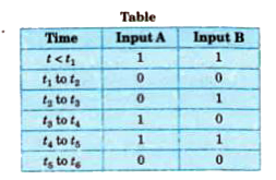
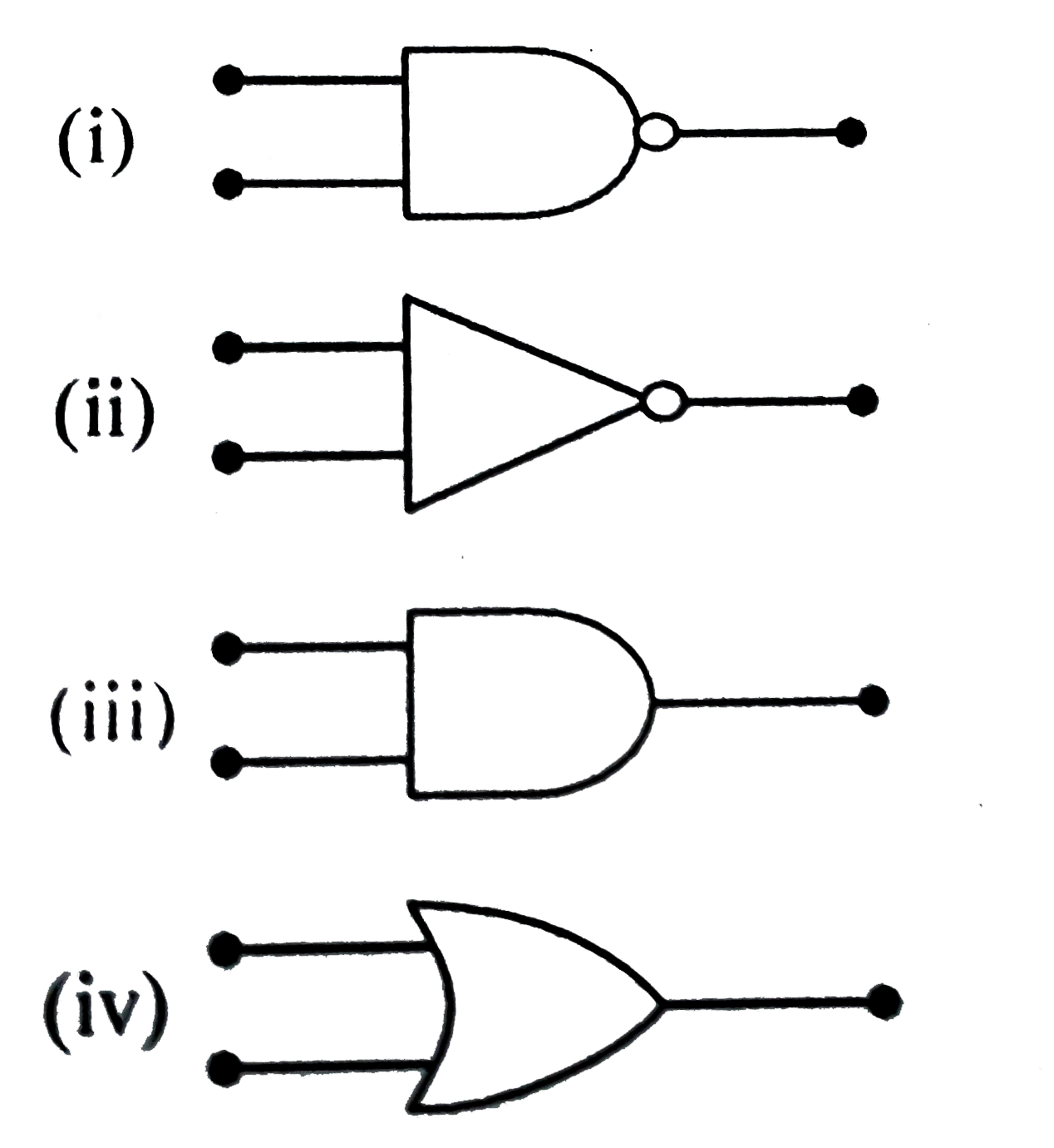
For a NAND gate the inputs and outputs for different time invervals are given below :
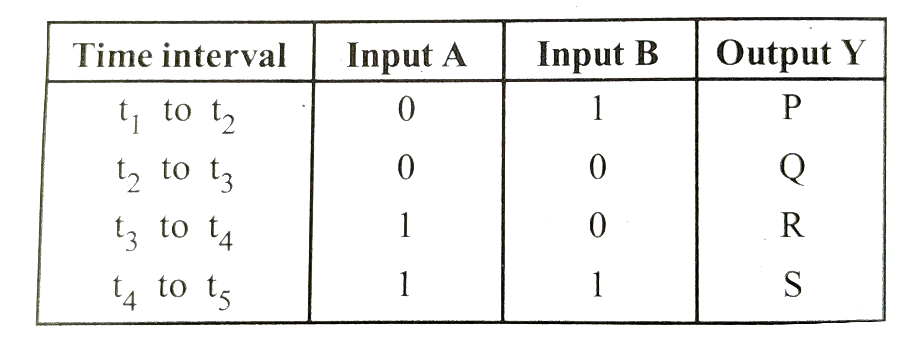
The values taken by P,Q,R,S are respectively
A
1,0,1,1
B
1,1,1,0
C
0,1,0,1
D
0,1,0,0
Video Solution
Text Solution
The correct Answer is:B
The truth table of the NAND gate is given as
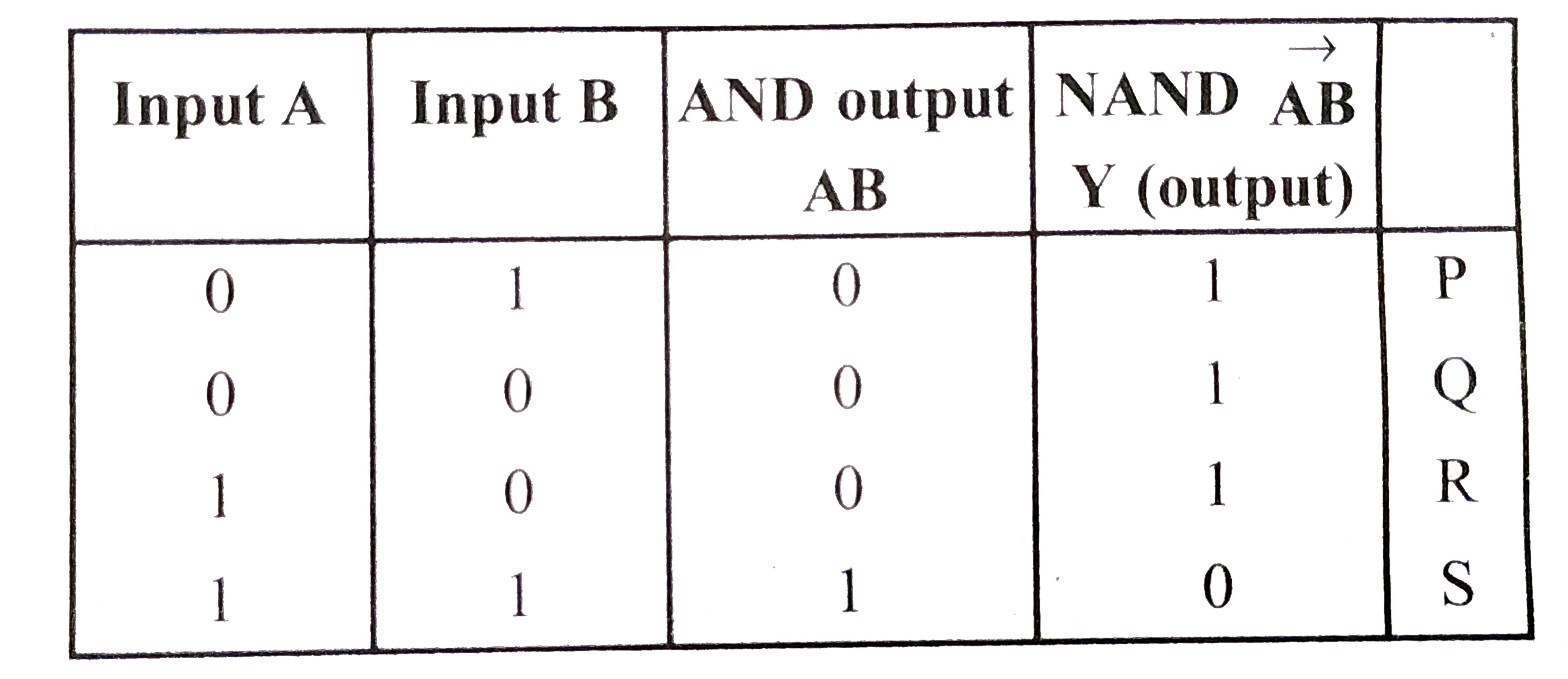
∴ The values of P,Q,R,S are (1,1,1,0)
|
Topper's Solved these Questions
Similar Questions
Knowledge Check
The inputs and outputs for different time intervals are given below for NAND gate
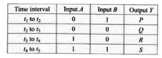
The value taken by P, Q, R, S are respectivelyA1,1,1,0B0,1,0,1C0,1,0,0D1,0,1,1If p→(q∧r) is false, then the truth values of p,q and r are respectively
AT,F and FBF,F and FCF, T and TDT,T and FA NOR gate and a NAND gate are connected shown. Two different sets of inputs are given to this set up. In the first case, the inputs to the gates are A = 0, B = 0, C = 0. In the second case, the inputs are A = 1, B = 0, C = 1. The output D in the first case and second case respectively are
 A0 and 0B0 and 1C1 and 0D1 and 1
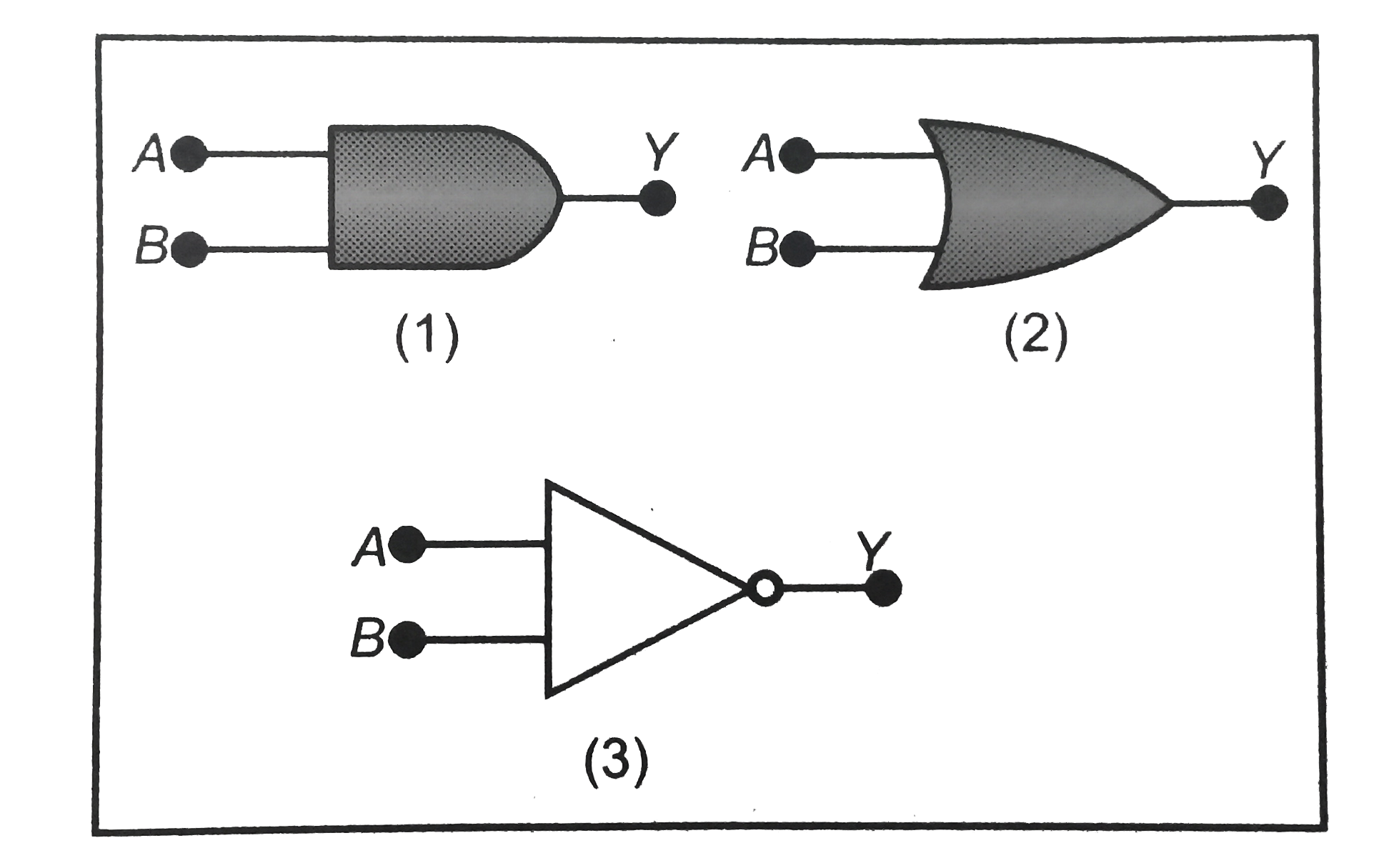
The symbolic representation of four logic gates are given below :

The logic symbols for OR, NOT and NAND gates are respectively :-
View SolutionLet a:~(p∧~r)∨(~q∨s)andb:(p∨s)lar(q∧r). If the truth values of p and q are true and that of r and s are false, then the truth values of a and b are respectively . . .
View SolutionGiven below are symbols for some logic gates :-
_E01_343_Q01.png)
The XOR gate and NOR gate respectively are :-
View SolutionGiven below are symbols for some gates. The OR gate and the AND gate, respectively are
View SolutionIf the truth value of the statement p→(~q∨r) is false (F), then the truth values of the statements p,q and r are respectively
View Solution


