Draw the schematic symbols for AND, OR, NOT and NAND gate.
Step by step video & text solution for Draw the schematic symbols for AND, OR, NOT and NAND gate. by Physics experts to help you in doubts & scoring excellent marks in Class 12 exams.
Updated on:21/07/2023Topper's Solved these Questions
- JULY 2016Book:GURUKUL PUBLICATION - MAHARASHTRA PREVIOUS YEAR PAPERSChapter: JULY 2016Exercise:SECTION -II
Explore 21 Videos
- FEBRUARY 2019Book:GURUKUL PUBLICATION - MAHARASHTRA PREVIOUS YEAR PAPERSChapter: FEBRUARY 2019Exercise:SECTION-D
Explore 6 Videos
- JULY 2017Book:GURUKUL PUBLICATION - MAHARASHTRA PREVIOUS YEAR PAPERSChapter: JULY 2017Exercise:SECTION-I
Explore 12 Videos
Similar Questions
Knowledge Check
NAND gate is-
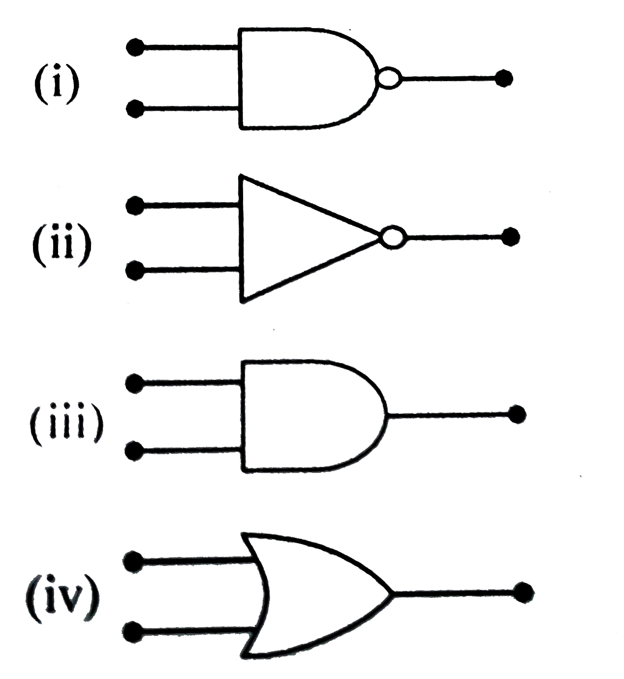
Aa basic gateBnot a universal gateCa universal gateDa universal gateThe symbolic representation of four logic gates are given in Fig.The logic symbol for OR, NOT and NAND gates are respectively
 A(iv), (i), (iii)B(iv), (ii), (i)C(i), (iii), (iv)D(iii),(iv), (ii)
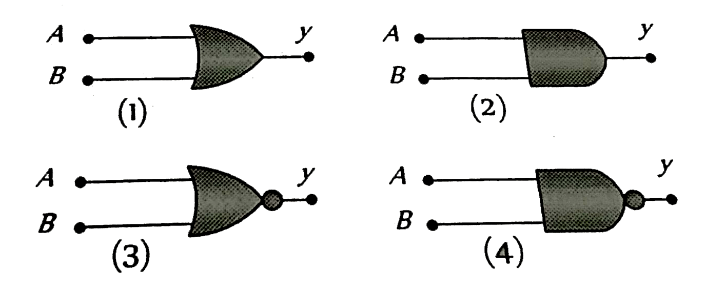
Given below are four logic gate symbol (figure). Those for OR, NOR and NAND are respectively
 A1,4,3B4,1,2C1,3,4D4,2,1
Give the logic symbol of AND gate.
View SolutionGiven below are four logic gates symbol (figure). Those for OR, NOR and NAND are respectively
View SolutionGive the logic symbol of NAND gate.
View SolutionDraw the logic symbol of NAND gate and give its Truth table
View Solution(a) Draw a neat diagram for a full wave rectifier circuit
(b) Draw the logic gate symbol and the truth table for a NAND gate with tow inputs
(c ) In an n-p-n tranasistor circuit the collector current is 10 mA if 95% of the enemitter current reach the collector what is the base current
View Solution


