Complete Solutions to EVALUATION QUESTIONS AND ANSWER of chapter SEMICONDUCTOR ELECTRONICS : MATERIALS , DEVICES AND SIMPLE CIRCUITS of Class 12 book with complete answers and questions
| Class 12 | PHYSICS |
| Chapter | SEMICONDUCTOR ELECTRONICS : MATERIALS , DEVICES AND SIMPLE CIRCUITS |
| NEW JOYTHI PUBLICATION | EVALUATION QUESTIONS AND ANSWER |
| Number Of Questions | 47 |
| Academic Year | 2023-24 |
The energy gap of diamond is 6 eV .
a . What does it mean ?
b. What is the value of energy gap in the case of copper ?
c. On the basis of energy gap , explain how substances are classified.
View SolutionWhen impurity (atom) is added to an intrinsic semiconductor , then it becomes extrinsic semiconductors .
What is the above process called ?
b. What is the advantage of doing so ?
c. Distinguish between intrinsic semiconductor and extrinsic semiconductor.
View SolutionFig shows a p-n junction diode.
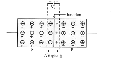
a. What does `V_(B)` denote ?
b. Name the region AB.
View SolutionWhat is the value of conductivity of a semiconductor at absolute zero ?
View SolutionCan a transistor amplifier generate power ?
View SolutionGive some properties of a semiconductor.
View SolutionWhat is a Zener diode ?
View SolutionWhat are the characteristics of a hole ?
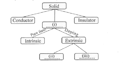
View SolutionCopy and complete the following block diagram .
View SolutionWhat is meant by forbidden energy gap ?
View SolutionWhat do you mean by fermi energy ?
View SolutionWhat is depletion region in p-n junction ?
View SolutionWhat will happen if both , emitter and collector of a transistor are reverse biased ?
View SolutionHow does conductivity of a semiconductor increase ?
View Solution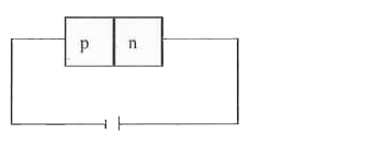
The forward bias of a diode is wrongly given above .
a. Redraw the above circuit correctly .
b. Draw the graph of current I with voltage V in forward bias .
c. Classify the following circuit diagram into forward bias , reverse bias , unbias

View SolutionClassify the following into conductors , insulators and semi conductors .
GaAs , InP , Ni, Calcite , Graphite
View SolutionThe magnitude of potential barrier of germanium is about 0.3 V .
a What does it mean . , b . What is the value of potential barrier for silicon ?
View Solution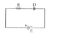
a. What type of biasting is used here ?
b. What happens to the depletion region ?
c. Will the diode conduct or not ?
View SolutionWhy is a NOT gate known as an inverter ?
View Solution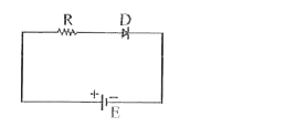
a. What type of biasting is used here ?
b. What happens to the depletion region ?
c. Will the diode conduct or not ?
View Solution
The above figures represent a p-n-p transistor and an n-p-n transistor.
a. Draw the circuit symbols of p-n-p transistor and n-p-n transistor .
b. Write the names of the terminals (1) , (2) and (3) .
View SolutionIn the normal working of a transistor , the emitter is forward biased and collector is reverse biased.
a. Comment on the above statement .
b. Can we exchange emitter and collector of a transistor ?
c. Base region of a transistor is made very thin and lightly doped. Why ?
d. "Eventhough the collector - base is reverse biased, the current flow takes place with out experiencing much high resistance" , Give your explanation.
View SolutionA transistor is being used as a common emitter amplifier .
a What is the phase relationship between the output and input voltages ?
b. Define voltage gain of an amplifier.
c. Define the transconductance of a transistor .
View SolutionHow does the conductivity of a semiconductor change with rise in temperature ? Explain.
View SolutionWhy are Ge and Si semiconductors ?
View SolutionWhy is a common emitter amplifier preferred over a common base amplifier ?
View Solution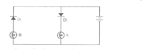
a . What do you observe when the circuit is closed ?
b. What will happen when the polarity of cell is reserved ? Why ?
View SolutionWhat are the different transistor configurations ?
View SolutionWhich configuration is widely used in circuits ?
View SolutionWhat is the name of the device in which AC is converted into DC ?
View SolutionWhat is the name of the device in which DC is converted into AC ?
View SolutionHow can you keep the LC oscillation undamped ?
View SolutionWhat the different gains in a transistor ?
View SolutionWhat is dark current ?
View SolutionTransistor Radio does not work satisfactorily when used inside a railway carriage .
a . Justify your answer .
b . What happens in a transistor when both the emitter and collector are reverse biased ?
c. What is this condition known as ?
d. Under what condition a transistor works as an open switch ?
View SolutionFill in the blanks with appropriate words given below .
[Base , collector , emitter , base-collector junction, collector - emitter junction , emitter base junction ]
Structurally a bipolar junction transistor consists of emitter , base and `underline"(i)"` Out of these regions `underline"(ii)"` is the most heavily doped. For proper functioning of a transistor. `underline"(iii)"` is forward biased and `underline"(iv)"` is reverse biased.
View SolutionA car stereo working at stabilized voltage supply of 9V DC and has a Zener diode of 9V , 0.25 W . But the voltage supply inside the car is 12 V DC .
The boy approached you to get help .
a. Which mode of bias will you suggest to connect Zener diode as voltage regulator ?
b. Draw a circuit diagram of voltage regulation to help the boy .
c . Which device is essential for circuit diagram ? Find the value of that device .
[ Hint . Current through the load , `I_(L) = 0`]
View SolutionState whether true or false and justify .
a Zener diodes are used under forward bias.
b. In n-p-n transistor , current conduction is primarily due to electrons .
c. Transistor amplifiers do not strictly obey law of conservation of energy since output power is greater than input power .
d. In a transistor amplifier all the frequency will have exactly equal gain .
View SolutionIn both p and n type semiconductors , actually electrons are flowing . What difference do you observe in the motion of electron in these two semiconductors ?
View SolutionA greenhouse has an electronic system (block diagram is given below ) which automatically switches ON a heater if the air temperature in the greenhouse drops too low . A manual switch is included so that the automatic system can be switched off .
(Hint , The temperature sensor gives a logic -I output when the air temperature is normal and logic 0 when it is too cold )

a. What is meant by 1 and 0 in digital circuit ?
b. Name the logic gate X . Why is it used ?
c. Name the logic gate Y.
d. Construct a truth table of this electronic system by taking A and B as inputs and D as output
View SolutionThe behaviour of the control unit of an automatic gas cooker is given below .

Cooking time is different by different dishes . Hence cooking time must be adjusted properly . This control unit can be constructed by using logic gates .
a . What is meant by logic gates ?
b . Which gate is suitable for the above control unit ?
c. Construct a simple circuit diagram of control unit (Using symbol of logic gate and block diagram of others)
View SolutionConstruct a truth table for the following logic circuit

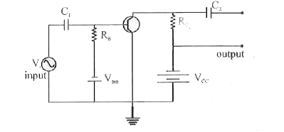
View SolutionCorrect the following CE amplifier circuit .
View Solution
a. Name the gates in the combination .
b. Identify the logic operation of the whole gate .
c. Give the truth table .
View SolutionCrystalline substances have a sharp melting point . Why ?
View SolutionWhy are NAND and NOR gate called universal gate ?
View SolutionWhy do crystalline state most stable ?
View Solution
EVALUATION QUESTIONS AND ANSWER questions and complete solutions for chapter SEMICONDUCTOR ELECTRONICS : MATERIALS , DEVICES AND SIMPLE CIRCUITS of NEW JYOTHI PHYSICS (TAMIL ENGLISH) of Class 12