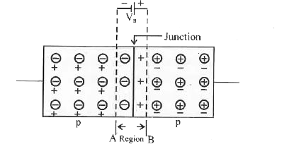
Fig shows a p-n junction diode.

a. What does VB denote ?
b. Name the region AB. Solution in Tamil
a. Potential barrier b. Depletion region
Topper's Solved these Questions
- SEMICONDUCTOR ELECTRONICS : MATERIALS , DEVICES AND SIMPLE CIRCUITS Book:NEW JOYTHI PUBLICATIONChapter:SEMICONDUCTOR ELECTRONICS : MATERIALS , DEVICES AND SIMPLE CIRCUITS Exercise:CONTINUOUS EVALUATION (ASSIGNMENT)
Explore 7 Videos
- SEMICONDUCTOR ELECTRONICS : MATERIALS , DEVICES AND SIMPLE CIRCUITS Book:NEW JOYTHI PUBLICATIONChapter:SEMICONDUCTOR ELECTRONICS : MATERIALS , DEVICES AND SIMPLE CIRCUITS Exercise:PREVIOUS YEAR QUESTIONS
Explore 3 Videos
- SEMICONDUCTOR ELECTRONICS : MATERIALS , DEVICES AND SIMPLE CIRCUITS Book:NEW JOYTHI PUBLICATIONChapter:SEMICONDUCTOR ELECTRONICS : MATERIALS , DEVICES AND SIMPLE CIRCUITS Exercise:PRACTICE PROBLEMS FOR SELF ASSESSMENT
Explore 8 Videos
- RAY OPTICS AND OPTICAL INSTRUMENTS Book:NEW JOYTHI PUBLICATIONChapter:RAY OPTICS AND OPTICAL INSTRUMENTS Exercise:COMPETITIVE EXAM CORNER
Explore 26 Videos
- WAVE OPTICSBook:NEW JOYTHI PUBLICATIONChapter:WAVE OPTICSExercise:COMPETITIVE EXAM CORNER
Explore 17 Videos
Similar Questions
On the basis of band theory , explain the difference between conductor , insulator and semiconductor.
View SolutionWe are familiar with the semi conductors Silicon and Germanium .
a. With a necessary schematic diagram , briefly explain the characteristics of an intrinsic semiconductor.
b. Draw the energy bands of a n-type semiconductor.
c The following figure represents a
d . Draw a typically illuminated P-n junctions solar cell.
e. LED convert............ energy to light.
View SolutionA semiconductor has the electron concentration 0.45×10¹²m−3 and hole concentration 5×1029m−3 . Find its conductivity . Given electron mobility = 0.135m2V−1s−1 and hole mobility = 0.048m2V−1s−1,e=1.6×10⁻¹⁹C
View SolutionA 100 W bulb produces an electric field of 2.9 V/m at a point 3m away. If the bulb is replaced by 400 W bulb without disturbing other conditions. Then the electric field produced at the same point is
View SolutionYoung's experiment is performed with light of wavelength 6000Å where in 16 frignes occupy a certain region on the screen. If 24 fringes occupy the same region with another light of wavelength λ then λ is
View SolutionIn a P−N junction diode is P region is heavily doped than n region then the depletion layer is
View SolutionIn the depletion region of an unbiased p-n junction diode, what are the charge carriers?
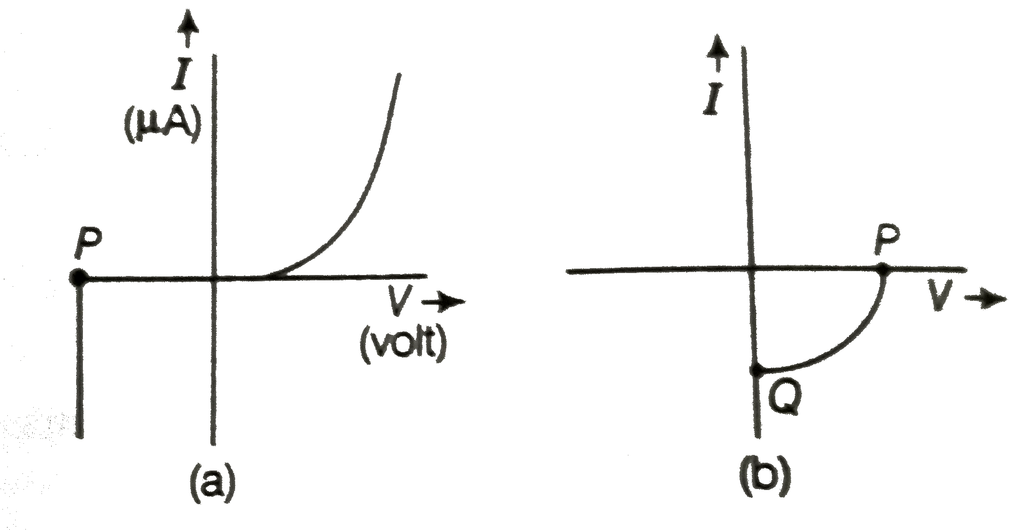
View Solution(i) Name the type of a diode whose characteristics are shown in figure (a) and (b) (ii) What does the point P in fig. (a) represent ? (iii) What does the point P and Q in fig. (b) represent ?
View SolutionIn the depletion region of an unbiased p-n junction diode there are
View SolutionWhat is a p-n junction diode?
Or,What is a junction diode?
View SolutionThe width of the depletion region in a P-N junction diode is
View SolutionIn the depletion region of an unbiased p-n junction diode, there are
View SolutionIn the depletion region of the an unbaised p-n junction diode, there are
View Solution(i) Name the type of a diode whose characteristics are shown in figure (a) and (b)
(ii) What does the point P in fig. (a) represent ?
(iii) What does the point P and Q in fig. (b) represent ?

View SolutionIn a p-n junction diode, holes diffuse from p-region to n- region because
View Solution

