Complete Solutions to COMPETITIVE EXAM CORNER of chapter SEMICONDUCTOR ELECTRONICS : MATERIALS , DEVICES AND SIMPLE CIRCUITS of Class 12 book with complete answers and questions
| Class 12 | PHYSICS |
| Chapter | SEMICONDUCTOR ELECTRONICS : MATERIALS , DEVICES AND SIMPLE CIRCUITS |
| NEW JOYTHI PUBLICATION | COMPETITIVE EXAM CORNER |
| Number Of Questions | 37 |
| Academic Year | 2023-24 |
A pure semiconductor has equal electron and hole concentration of `10^(16) m^(-3)` . Doping by indium increases `n_(h)` to `5 xx 10^(22) m^(-3)` . Then the value of `n_(e)` in the doped semiconductor is
View SolutionThe collector supply voltage is 6 V and the voltage drop across a resistor of `600 Omega` in the collector circuit is 0.6 V , in a transistor connected in common emitter mode . If the current gain is 20 , the base current is
View SolutionA full - wave rectifier circuit with an ac input is shown.

The output voltage across `R_(L)` is represented as
View SolutionWhen the voltage drop across a p-n junction diode is increased from 0.65 V to 0.70 V , the change in the diode current is 5 mA . The dynamic resistance of the diode is
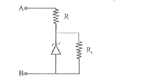
View SolutionIf the voltage between the terminals A and B is 17 V and Zener breakdown voltage is 9 V , then the potential across R is
View SolutionGaAs (with a band gap = 1.5 eV) as a L.E.D can emit
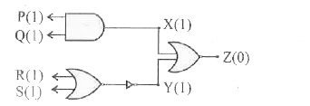
View SolutionThe circuit diagram shows a logic combination with the states of outputs X , Y and Z given for inputs P , Q , R and S all at state 1 . When inputs P and R change to state 0 with inputs Q and S still at 1 , the states of outputs X , Y and Z changes to
View SolutionIn a common emitter transistor amplifier , the output resistance is `500 k Omega` and the current gain `beta` = 49 . If the power gain of the amplifier is `5 xx 10^(6)` , the input resistance is
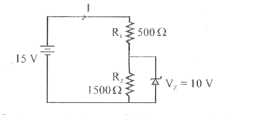
View SolutionIn the circuit given , the current through the zener diode is
View SolutionA transistor oscillator is (i) an amplifier with positive feedback (ii) an amplifier with reduced gain (iii) the one in which dc supply energy is converted into ac output energy . Then
View SolutionA semiconductor with a band gap of 2.5 eV is used to fabricate a p-n photodiode . It can detect a signal of wavelength
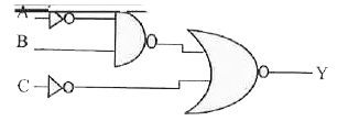
View SolutionIn the circuit given A , B and C are inputs and Y is the output

The output Y is
View SolutionIn the given circuits for ideal diode , the current through the battery is
View SolutionThe logic gates giving output '1' for the inputs of '1' and '0' are
View SolutionIdentify the mismatch of the following :

View SolutionIf a PN junction diode of depletion layer width W and barrier height `V_(0)` is forward biased , then
View SolutionThe heavily and lightly doped regions of a bipolar junction transistor are respectively
View SolutionThe device used for detecting optical signal is
View Solution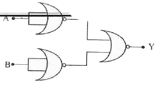
The logical operation carried out by the above circuit is
View SolutionIn CE transistor amplifier , if the base current is increased by 20 `mu` A , the collector current changes from 4 mA to 5 mA . The current amplification factor of the transistor is
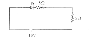
View SolutionIf an ideal junction diode is connected as shown , then the value of the current iis

View SolutionIdentify the mismatched pair from the following
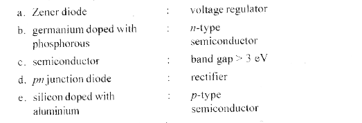
View SolutionIn a common emitter configuration a transistor has `beta = 50` and input resistance`1 k Omega`. If the peak value of a.c. input is `0.01` V , then the peak value of collector current is
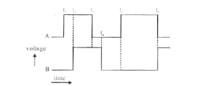
View SolutionThe wave forms A and B given below are given as input to a NAND gate . Then its logic output y is
View SolutionThe output of an AND gate is connected to both the inputs of a NOR gate , then this circuit will act as a
View SolutionIn p-type semiconductor , the acceptor level lies
View SolutionIf the feedback voltage is increased in a negative feedback amplifier , then
View SolutionThe inputs A , B and C to be given in order to get an output Y = 1 from the following circuit are

View SolutionThe collector resistance and the input resistance of a CE amplifier are respectively `10 kOmega` and `2 k Omega` . If `beta` of the transistor is 49 , the voltage gain of the amplifier is
View SolutionThe light emitting diode (LED) is
View SolutionIdentify the wrong statement
View SolutionIdentify the wrong statement with reference to a solar cell
View SolutionThe minimum number of NAND gates used to construct an OR gate is
View SolutionFor which one of the following input combinations , the given logic circuit gives the output Y = 1 ?
View SolutionIn a semiconductor `(2)/(3)` rd of the total current is carried by electrons and remaining `(1)/(3)` rd by the holes . If at this temperature , the drift velocity of electrons is 3 times that of holes , the ratio of number density of electrons to that of holes is
View SolutionIn an PNP transistor , `10^(10)` holes enter the emitter in `10^(-6)` s . If 2 % of holes is lost in the base , then the current amplification factor is
View SolutionThe electrical conductivity of a semiconductor increases when electromagnetic radiation of wavelength shorter than 600 nm is incident on it . The energy band gap (in eV) for the semiconductor is
View Solution
COMPETITIVE EXAM CORNER questions and complete solutions for chapter SEMICONDUCTOR ELECTRONICS : MATERIALS , DEVICES AND SIMPLE CIRCUITS of NEW JYOTHI PHYSICS (TAMIL ENGLISH) of Class 12