Complete Solutions to MCQ of chapter SEMICONDUCTOR ELECTRONICS : MATERIALS , DEVICES AND SIMPLE CIRCUITS of Class 12 book with complete answers and questions
| Class 12 | PHYSICS |
| Chapter | SEMICONDUCTOR ELECTRONICS : MATERIALS , DEVICES AND SIMPLE CIRCUITS |
| NCERT FINGERTIPS | MCQ |
| Number Of Questions | 100 |
| Academic Year | 2023-24 |
At absolute zero , Si acts as
View SolutionIn good conductors of electricity, the type of bonding that exists is
View SolutionThe manifestation of band structure in solids is due to
View SolutionCarbon , silicon and germanium have four valence elcectrons each . These are characterised by valence and conduction bands separated by energy band - gap respectively equal to ` (E_g)_(c) (E_g)_(si) ` and ` (E_g)_(Ge) `. Which of the following statements ture ?
View SolutionIf the energy of a photon of sodium light ( `lambda`=589 nm) equals the band gap of semiconductor, the minimum energy required to create hole electron pair
View SolutionThe electrical conductivity of a semiconductor increases when electromagnetic radiation of wavelength shorter than `2480 nm` is incident on it. The band gap in `(eV)` for the semiconductor is.
View SolutionFind the wavelength of light that may excite an electron in the valence band of diamond to the conduction band. The energy gap is 5.50 eV
View SolutionThe maximum wavelength of electromagnetic radiation, which can create a hole-electron pair in germanium. (Given that forbidden energy gap in germanium is 0.72 eV)
View SolutionThe probability of electrons to be found in the conduction band of an intrinsic semiconductor at a finite temperature
View SolutionWhich of the following equations correctly represents the temperature variation of energy gap between the conduction and valence bands for Si?
View SolutionAn intrinsic semiconductor has a resistivity of 0.50 `Omega` m at room temperature. Find the intrinsic carrier concentration if the mobilities of electrons and holes are `0.39 m^2 V^(-1) s^(-1)` and `0.11 m^2 V^(-1) s^(-1)` respectively
View SolutionIn pure semiconductor, the number of conduction electrons is `6 xx 10^18` per cubic metre. How many holes are there in a sample of size 1 cm x 1 cm x 1 mm?
View SolutionMobilities of electorns and holes in a sample of intrinsic germanium at room temperature are `0.54m^(2)V^(-1)s^(-1)` and `0.18m^(2)V^(-1)s^(-1)` respectively.
If the electron and hole densities are equal to `3.6xx10^(19)m^(-3)` calculate the germanium conductivity.
View SolutionA block of pure silicon at `300 K` has a length of `10 cm` and an area of `1.0 cm^(2)`. A battery of emf `2V` is connected across it. The mobility of electron is `0.14 m^(2) v^(-1) S^(-1)` and their number density is `1.5 xx 10^(16) m^(-3)`. The mobility of holes is `0.05 m^(2) v^(-1) S^(-1)`.
The electron current is
View SolutionIn an n- type silicon, which of the following statements is true ?
(a) Electrons are majority carries and trivalent atoms are the dopants.
(b) Electrons are majority carries and pentavalent atoms are the dopants.
(c ) Holes are minority carries and paentavalent atoms are the dopants.
(d) Holes are minority carries and trivalent atoms are the dopants.
View SolutionIf a small amount of antimony is added to germanium crystal
View SolutionIn n-type semiconductor when when all donor states are filled, then the net charge density in the donor states becomes
View SolutionSuppose a pure Si-crystal has `5xx10^(28) "atoms" m^(-3)`. It is doped by 1 ppm concentration of pentavalent As. Calculate the number of electrons and holes. Give that `n_(i)=1.5xx10^(16)m^(-3)`.
View SolutionA semiconductor has equal electron and hole concentration of `6xx10^(8)//m^(3)`. On doping with certain impurity, electron concentration increases to `9xx10^(12)//m^(3)`. (i) Identify the new semiconductor obtained after doping. (ii) Calculate the new hole concentration. (iii) How does the energy gap vary with doping?
View SolutionThe number density of electrons and holes in pure silicon at `27^@` C are equal and its value is `2.0 xx 10^16 m^(-3)`. On doping with indium the hole density increases to `4.5xx 10^22 m^(-3)`, the electron density in doped silicon is
View SolutionThe dominant mechanisms for motion of charge carriers in forward and reverse biased silicon `P-N` junction are
View SolutionIn an unbiased p-n junction electrons diffuse from n-region to p-region because :-
View SolutionRegion which have no free electron and holes in P-N junction is
View SolutionIn the depletion region of a diode.
View SolutionIn a `p-n` junction diode, the barrier potential opposes diffusion of
View SolutionA potential barrier of 0.3 V exists across a p-n junction. If the depletion region is 1 `mu`m wide, what is the intensity of electric field in this region?
View SolutionWhich of the junction diodes shown below are forward biased ?
View SolutionA forward biased diode is
View SolutionWhen the voltage drop across a `p.n` junction diode is increased from `0.65V` to `0.70V`, the change in the diode current is `5mA`. What is the dynamic resistance of the diode?
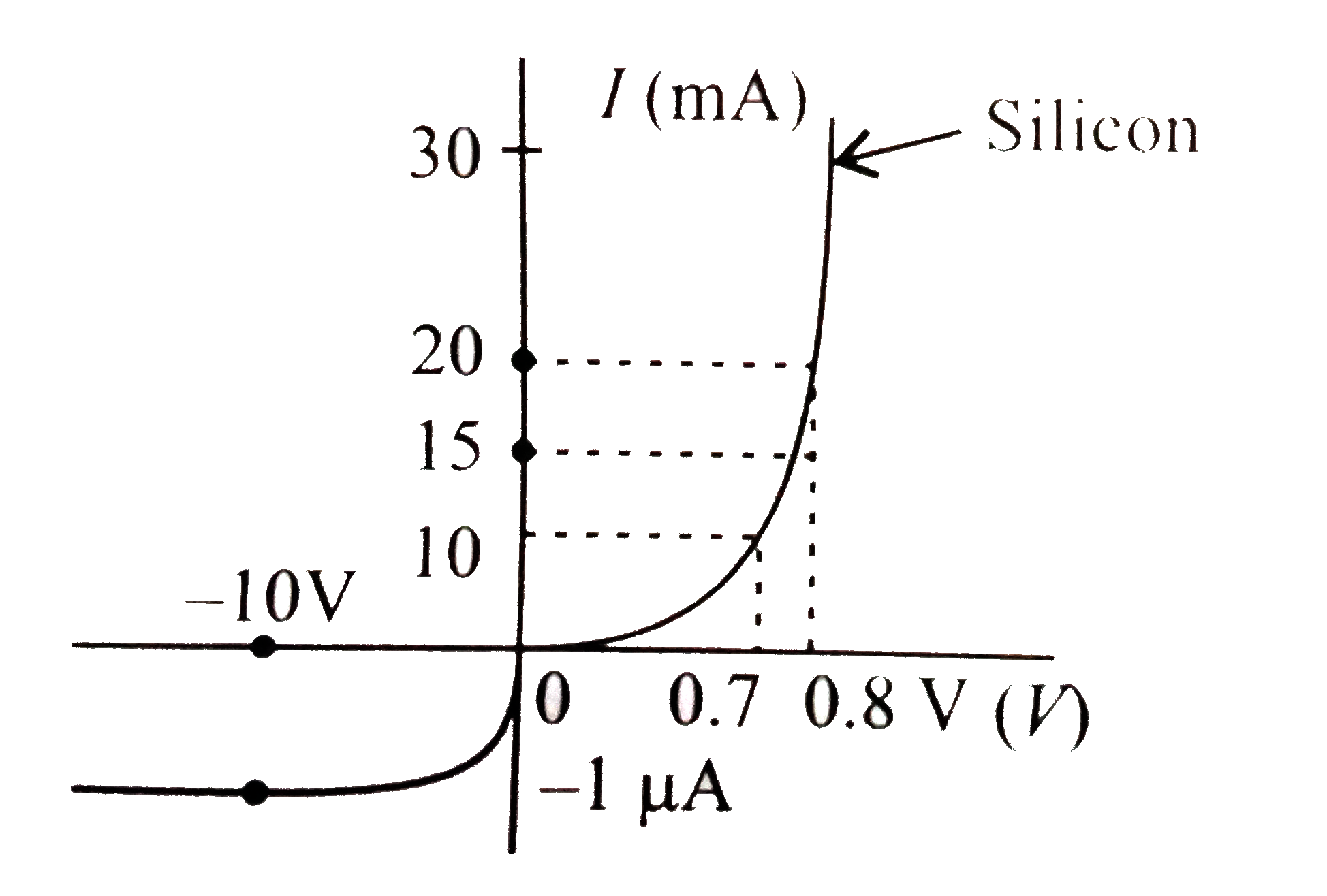
View SolutionThe V-I characteristic of a silicon diode is shown in figure . The resistance of the diode at `I_D`=15 mA is
View SolutionThe breakdown in a reverse biased p-n junction diode is more likely to occur due to
View Solution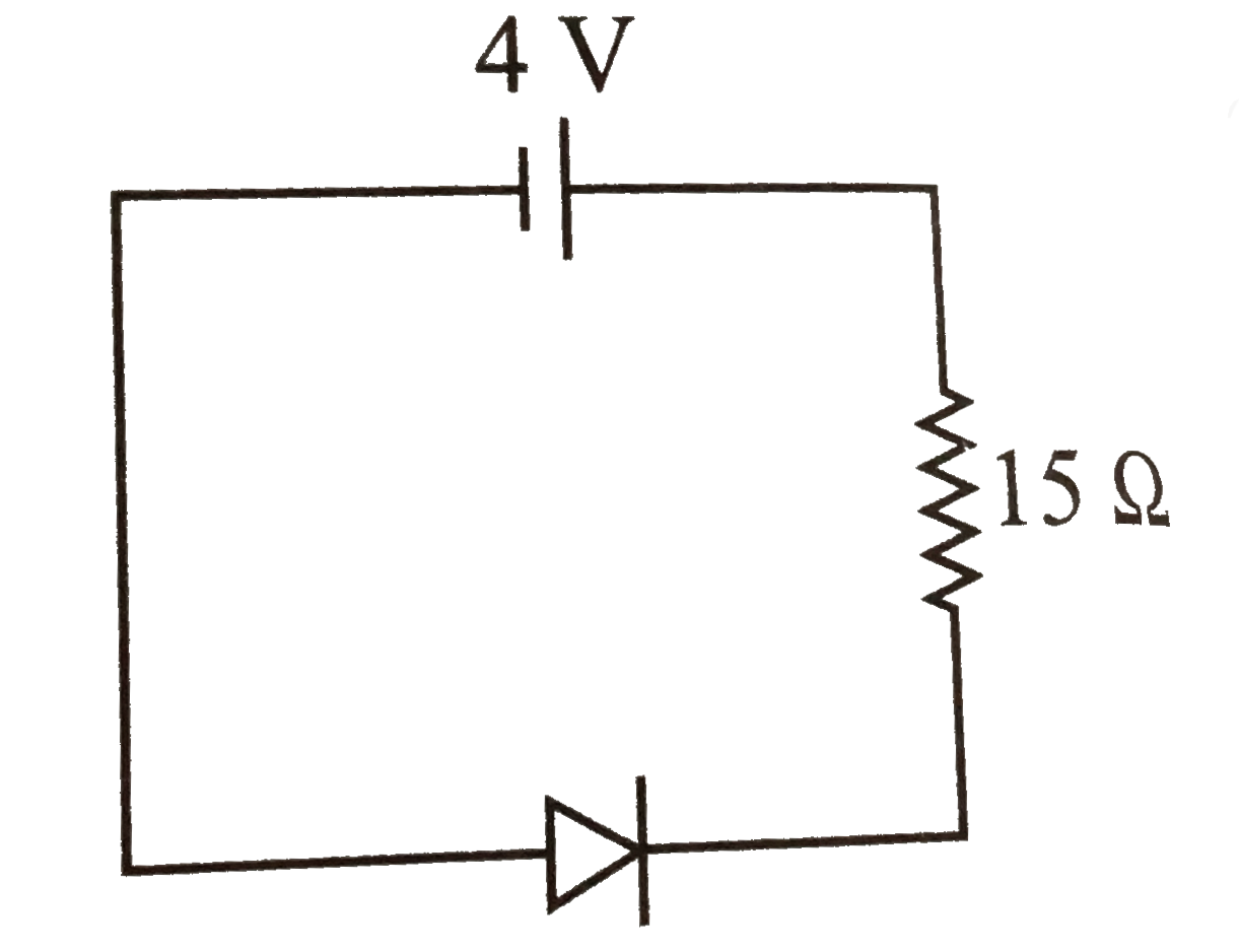
In the circuit shown if current for the diode is `20 muA`, the potential difference across the diode is
View SolutionOf the diodes shown in the following figures, which one is reverse biased ?
View SolutionThe equivalent resistance of the circuit shown in figure between the points A and B if `V_A lt V_B` is
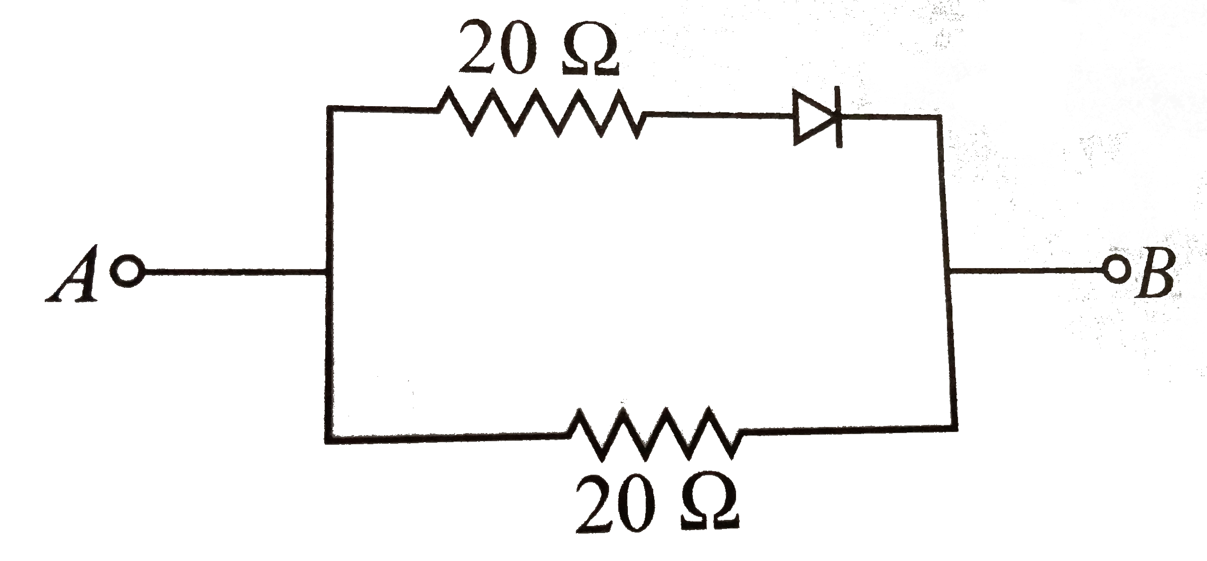
View SolutionThe equivalent resistance between the points A and B, if `V_A gt V_B` is
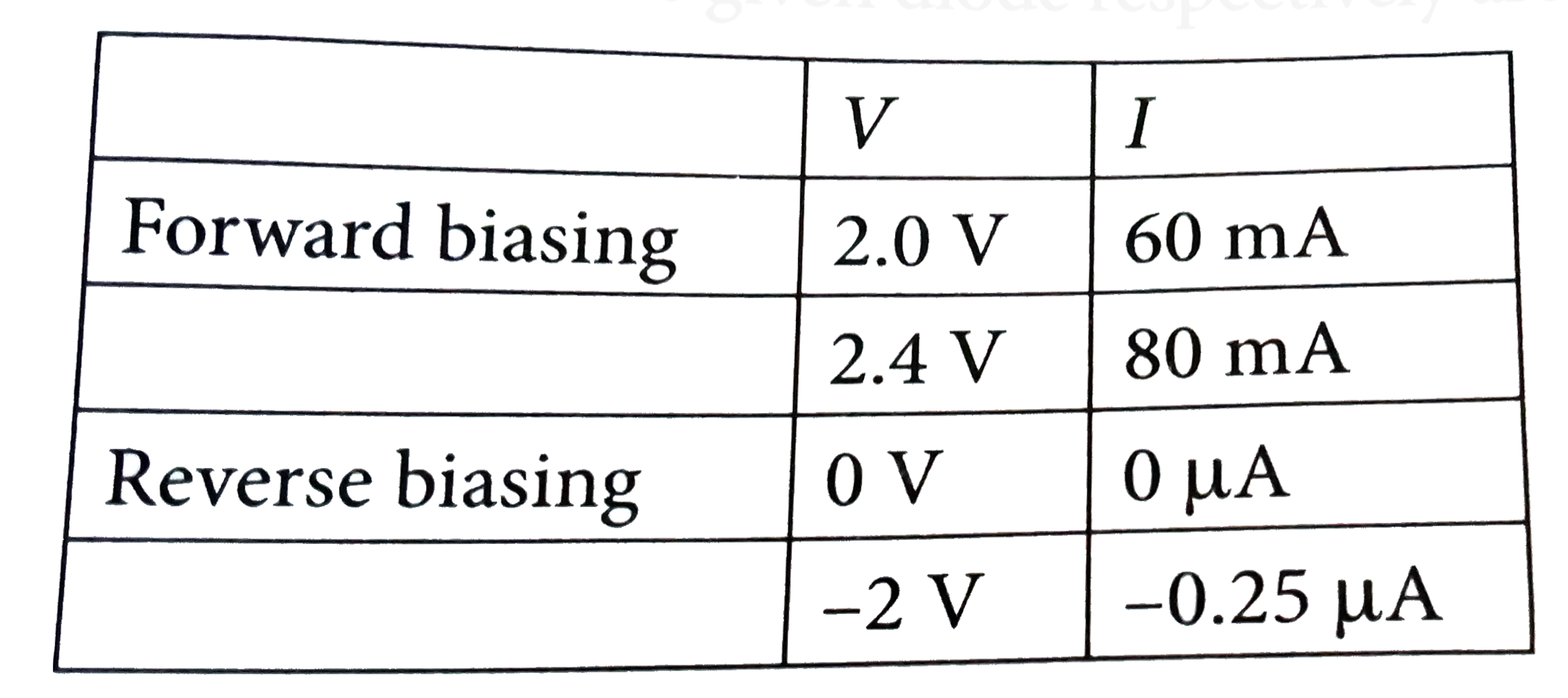
View SolutionThe following table provides the set of values of V and I obtained for a given diode. Let the characteristics `alpha` be nearly linear, over this range, the forward and reverse bias resistance of the given diode respectively are
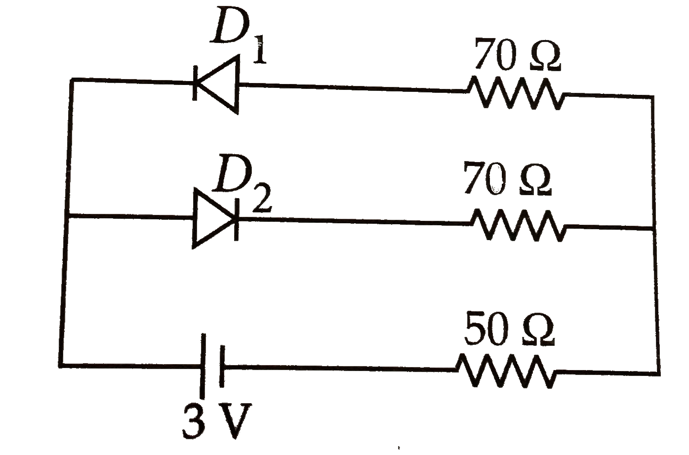
View SolutionThe circuit shown in the figure contains two diodes each with a forward resistance of 30 `Omega` and with infinite backward resistance. If the battery is 3 V, the current through the 50 `Omega` resistance (in ampere) is
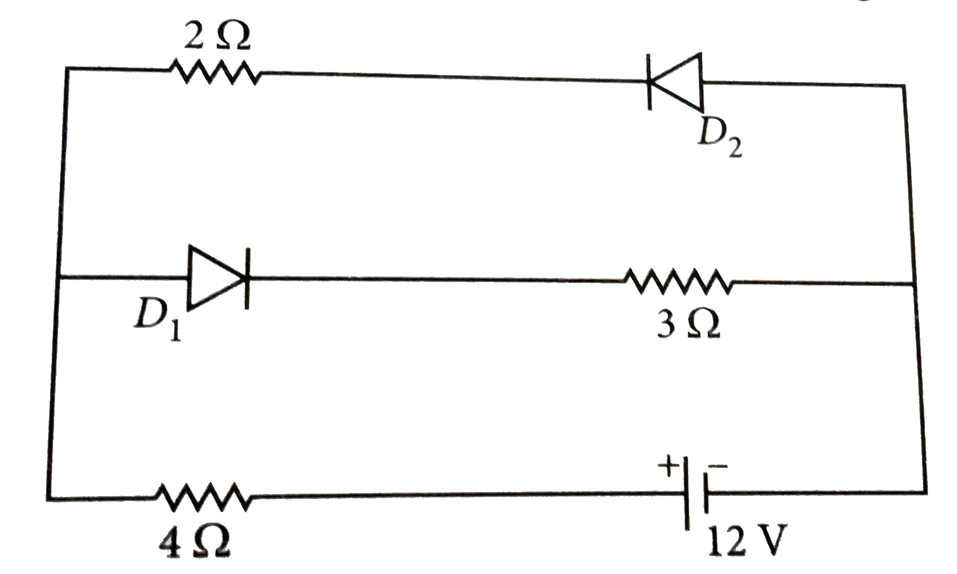
View SolutionThe circuit has two oppositely connected ideal diodes in parallel. What is the current flowing in the circuit?
View SolutionIn a full wave rectifier circuit operating from `50 Hz` mains frequency , the fundamental frequency in the ripple would be
View SolutionIn a full wave junction diode rectifier, the input a.c. has r.m.s. value of 20 V. The transformer used is a step up transformer having primary and secondary turns ratio 1: 2. Calculate the d.c. voltade in the recitified output.
View SolutionIn a half wave rectifier circuit operating from 50 Hz mains frequency, the fundamental frequency in the ripple would be
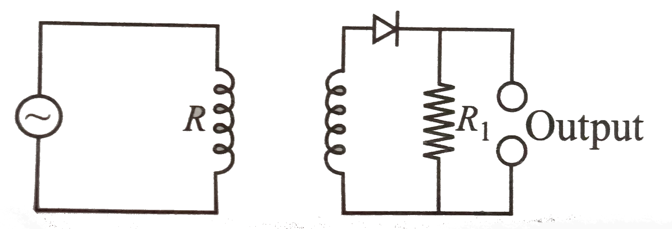
View SolutionA sinusoidal voltage of rms value 220 V is applied to a diode and a resistor R in the circuit shown in figure so that half wave rectification occurs. If the diode is ideal, what is the rms voltage across `R_1`?
View SolutionWhich of the following circuits provides full wave rectification of an ac input?
View SolutionWhat happens during regualtion action of a Zener diode?
View SolutionA Zener diode is specified having a breakdown voltage of 9.1 V with a maximum power dissipation of 364 mW. What is the maximum current that the diode can handle.
View SolutionIn the circuit, Fig The current through the zener diode is
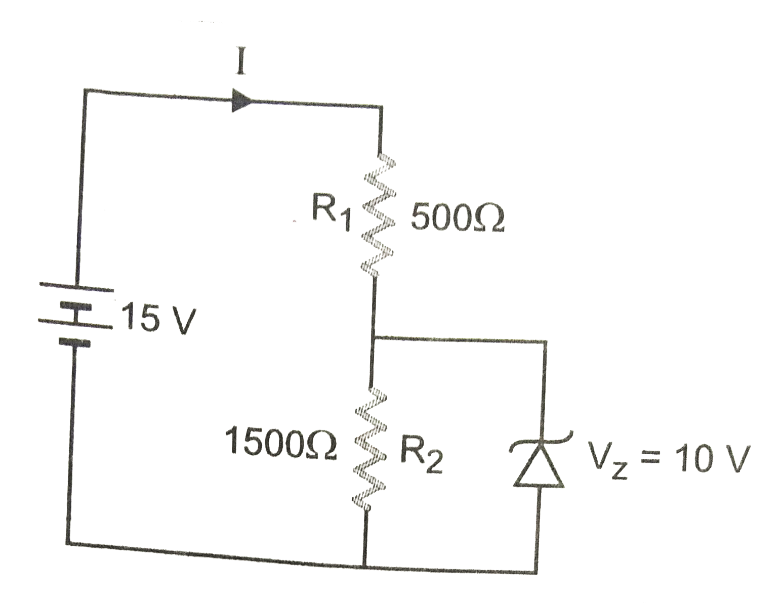
View SolutionFrom the Zener diode circuit shown in figure, the current through the Zener diode is
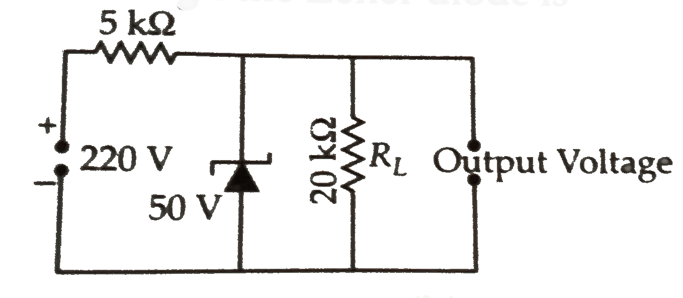
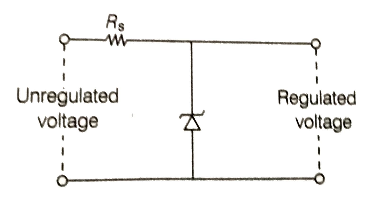
View SolutionA Zener of power rating 1 W is to be used as a voltage regulator. If Zener has a breakdown of 5V and it has to regulate voltage which fluctuated between 3 V and 7 V, what should be the value of `R_(s)` for safe operation (see figure) ?
View SolutionA p-n photodiode is made of a material with a band gap of 2 e V. The minimum frequency of the radiation that can be absorbed by the material is nearly
(hc= 1240 eV nm)
View SolutionA `p-n` photodiode is fabricated from a semiconductor with a band gap of `2.5 eV`. It can detect a signal of wavelength
View SolutionThree photodiodes `D_1 , D_2 ` and `D_3` are made of semiconductors having
band gaps of ` 2.5 eV , 2 eV` and 3 eV , respectively . Which one will be able to detect light of wavelength ` 6000 Å ` ?
View SolutionThe transfer characteristics of a base biased transistor has the operation regions, namely, cutoff, active region and saturation region. For using the transistor as an amplifier it has to operate in the
View SolutionThe emitter of transistor is doped the heaviest because it
View SolutionThe heavily and lightly doped regions of a bipolar junction transistor are respectively
View SolutionFor a transistor amplifier, the voltage gain
View SolutionAn oscillator is nothing but an amplifier with
View SolutionThe current amplification factor `alpha` of a common base transistor and the current amplification factor `beta`of a common emitter transistor are not related by
View SolutionIf `beta, R_L and r` are the ac current gain, load resistance and the input resistance of a transistor respectively in CE configuration, the voltage and the power gains respectively are
View SolutionIf `alpha and beta` are the current gain in the CB and CE configurations respectively of the transistor circuit, then `(beta-alpha)/(alphabeta)=`
View SolutionA transistor has a current amplification factor (current gain) of 50. In a common emitter amplifier circuit, the collector resistance is chosen as `5Omega` and the input resistance is `1Omega`. The output voltage if input voltage is 0.01 V is
View SolutionTwo amplifiers are connected one after the other in series (cascaded). The first amplifier has a voltage gain of 10 and the second has a voltage gain of 20 . If the input signal is 0.01 V , calculate the output AC signal .
View SolutionThe amplifiers `X, Y` and `Z` are connected in series. If the voltage gains of `X, Y` and `Z` are `10, 20` and `30`, respectively and the input signal is `1mV` peak value, then what is the output signal voltage (peak value)
(i) if dc supply voltage is 10V ?
(ii) if dc supply voltage is 5V?
View Solutionwhat is the output signal voltage (peak value) if dc supply voltage is 5 V?
View SolutionIn n-p-n transistor circuit, the collector current is `10 mA`. If `90%` of the holes reach the collector, find emitter and base currents.
View SolutionA transistor connected in common emitter mode, the voltage drop across the collector is 2 V and `beta` is 50, the base current if `R_C` is `2 kOmega` is
View SolutionThe power gain for common base amplifier is 800 and the voltage amplification factor is 840. The collector current when base current is 1.2 mA is
View SolutionThe current gain for a common emitter amplifier is 69. If the emitter current is 7 mA, the base current is
View SolutionThe potential difference across the collector of a transistor, used in common emitter mode is 1.5 V, with the collector resistance of `3 kOmega`, the emitter current is [`beta= 50`]
View SolutionIn a common -emitter transistor amplifier, an increase of `50muA` in the base current causes an increase of `1.0mA` in the collector current . Calculat gain `beta`. What will be the change in emitter current? Also calculate current gain `alpha`
View SolutionFor a common emitter transistor amplifier, the audio signal voltage across the collector resistance of `2 kOmega` is 2 V. Suppose the current amplification factor of the transistor is 100, the base current if base resistance is `1 k Omega` is
View SolutionThe ac current gain of a transistor is 120. What is the change in the collector current in the transistor whose base current changes by `100 muA`?
View SolutionIn an n-p-n circuit transistor, the collector current is 10 mA. If 80% electrons emitted reach the collector, then
View SolutionA common emitter amplifier gives an output of 3 V for an input of 0.01 V. If `beta` of the resistance is 100 and the input resistance is `1 kOmega`. then the collector resistance is
View SolutionThe input resistance of a common emitter transistor amplifier, if the output resistance is `500 kOmega`, the current gain `alpha=0.98` and the power gain is `6.0625 xx 10^(6)` is
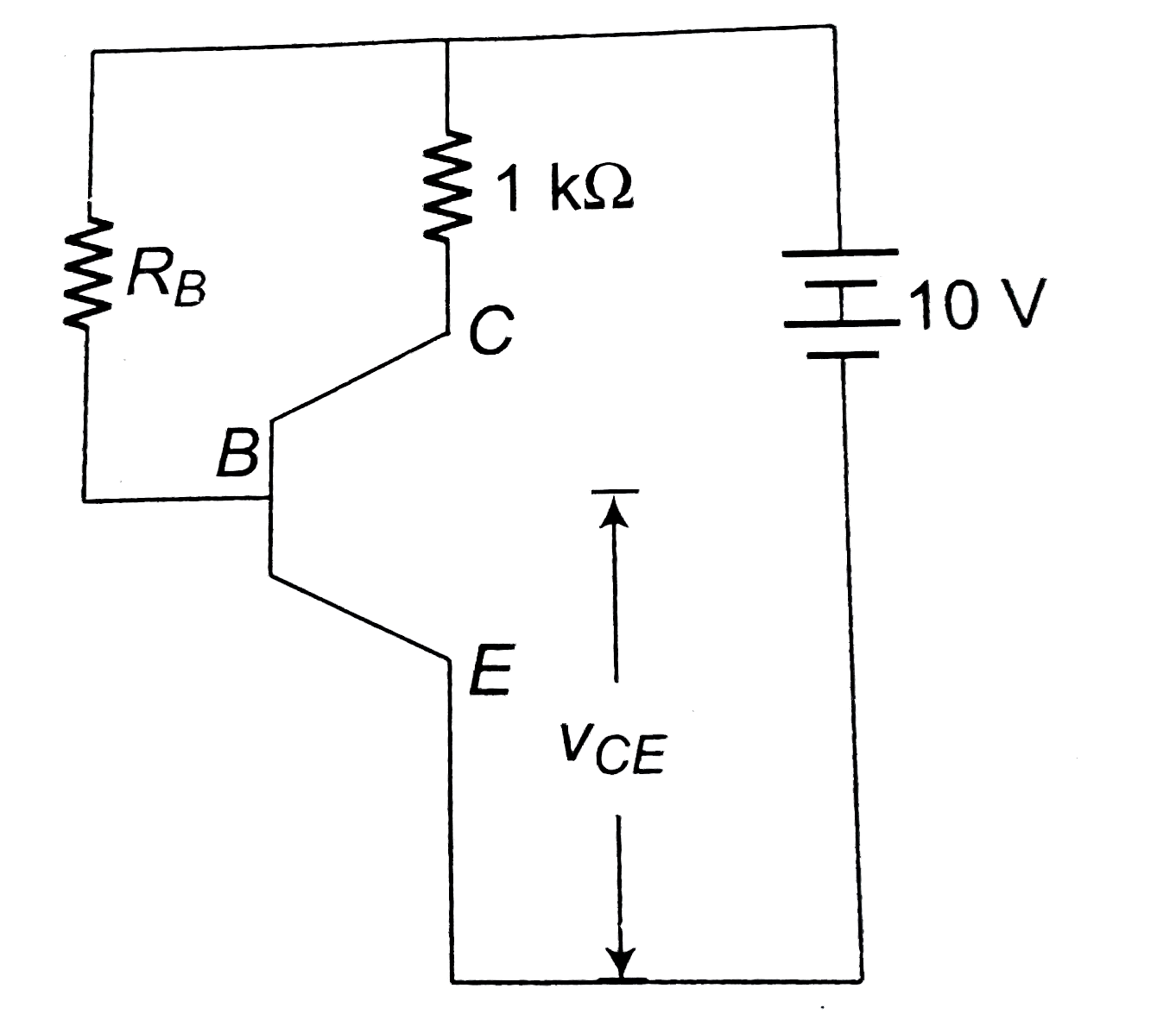
View SolutionIn the cuircuit shown here the transistor used has a current gain `beta=100`. What should be the bias resistor `R_(BE)` so that `V_(CE)=5V("neglect "V_(BE))`
View SolutionThe input resistance of a transistor is `1000 Omega` on charging its base current by `10 muA`, the collector current increases by 2 mA. If a load resistance of `5 kOmega` is used in the circuit, the voltage gain of the amplifier is
View SolutionA transistor has a current gain of 30. If the collector resistance is `6kOmega`, input resistance is `1kOmega`, calculate its volage gain?
View SolutionIn a transistor connected in a common emitter mode `R_C = 4kOmega, R_1 = 1kOmega, I_C = 1mA` and `I_B = 20 muA`. Find the voltage gain.
View SolutionIn an n-p-n transistor `10^(10)` electrons enter the emitter in `10^(-6)`s. If 2% of the electrons are lost in the base, find the current transfer ratio and the current amplification factor.
View SolutionIf a change of `100 mu A` in the base current of an `n-p-n` transistor in `CE` causes a change of `10 mA` in the collector current, the `ac` current gain of the transistor is
View SolutionWhat is the voltage gain in a common emitter amplifier, where input resistance is `3Omega` and load resistance `24Omega` and `beta=61` ?
View SolutionAn amplifier has a voltage gain of 100. The voltage gain in dB is
View SolutionA transistor is operated in common emitter configuration at `V_C=2 V`. Such that a change in the base current from `100 muA` to `200 muA` produces a change in the collector current of 5mA to 10 mA. The current gain is
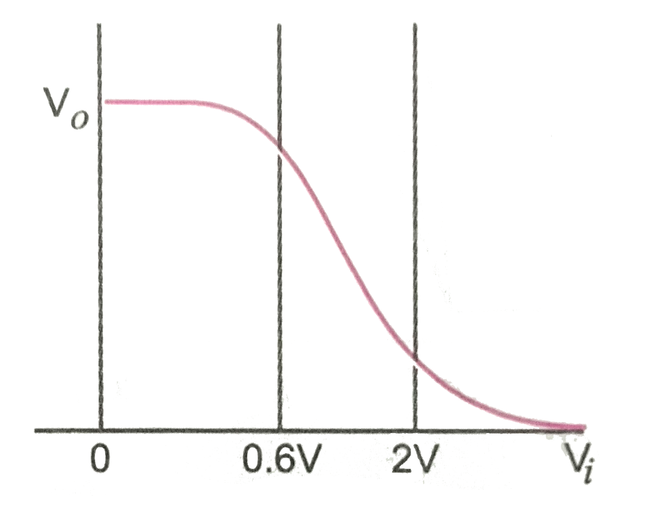
View SolutionFig.shows that transfer characteristics of a base biased CE transistor. Which of the following statements are true?
View SolutionBoolean algebra is essentially based on
View SolutionThe symbolic representation of four logic gates are given in Fig.The logic symbol for OR, NOT and NAND gates are respectively

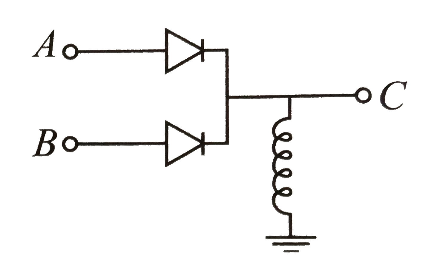
View SolutionIn the circuit below, A and B represents two inputs and C represents the output . The circuit represents
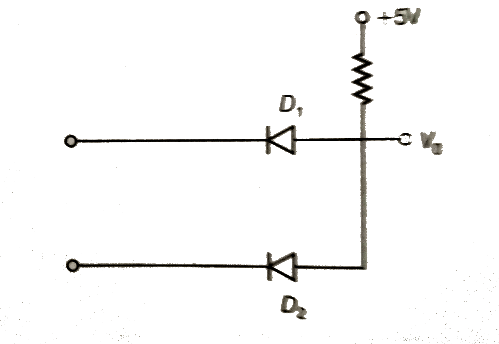
View SolutionWrite the truth table for the circuit shown in figure given below. Name the gate that the circuit resembles.
View SolutionIn boolean algebra, if `A=1` and `B=0` then the value of `A+barB` is
View SolutionWhat will be the input of `A` and `B` for the Boolean expression `bar((A+B)).bar((A.B))=1`?
View SolutionThe circuit given in figure, is equivalent to

View SolutionThe combination of NAND gates is shown in figure.The equivalent circuit is
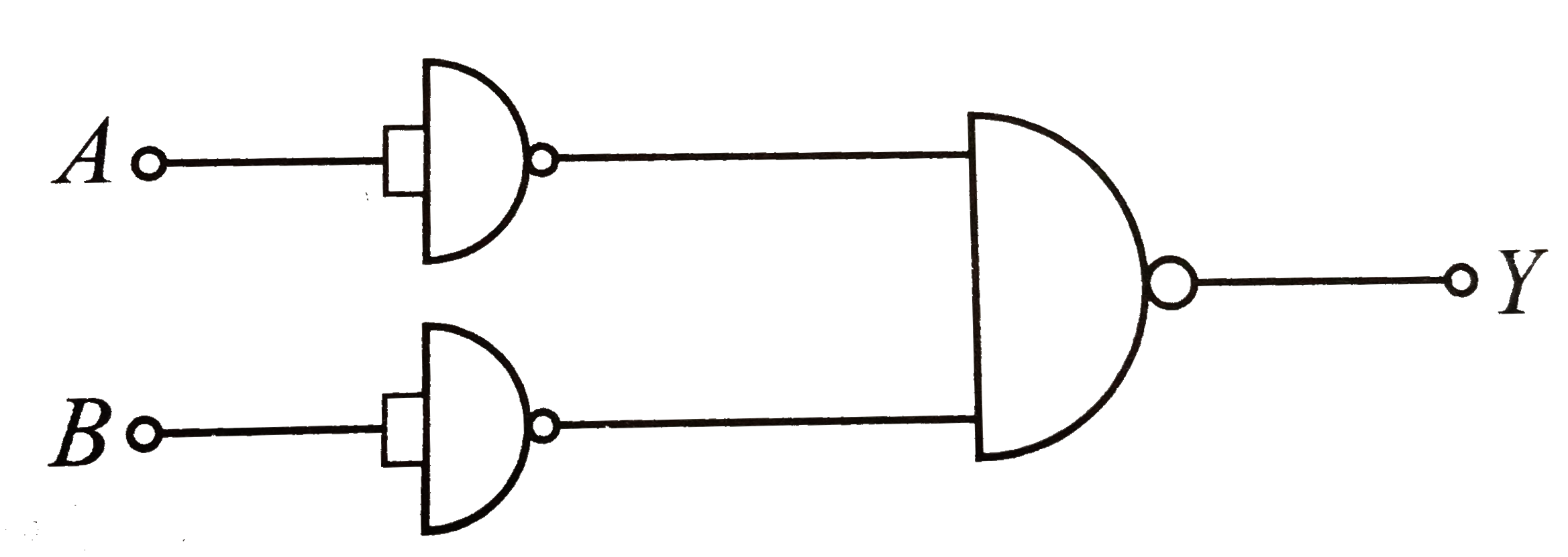
View SolutionThe diagram of a logic circuit is given below. The output `F` of the circuit is represented by
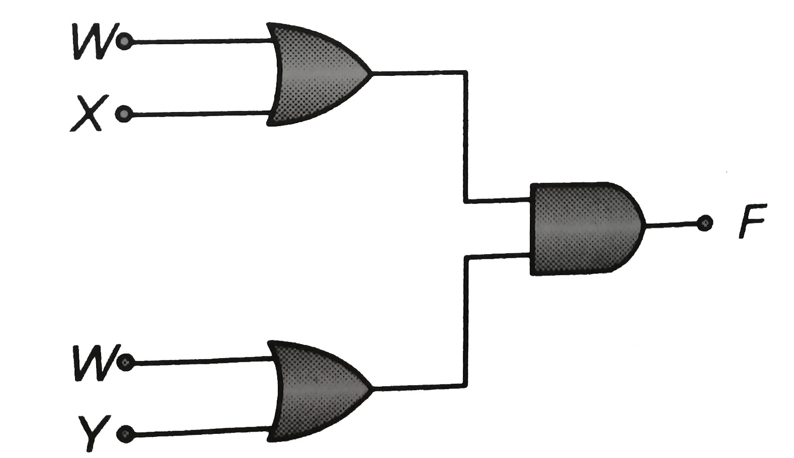
View Solution
The truth table of the logic circuit shown-
View SolutionSelect the outputs Y of the combination of gates shown below for inputs `A = 1,B = 0 , A = 1,B = 1` and `A = 0,B=0` respectively :-
_E01_437_Q01.png)
View SolutionThe given truth table is for which
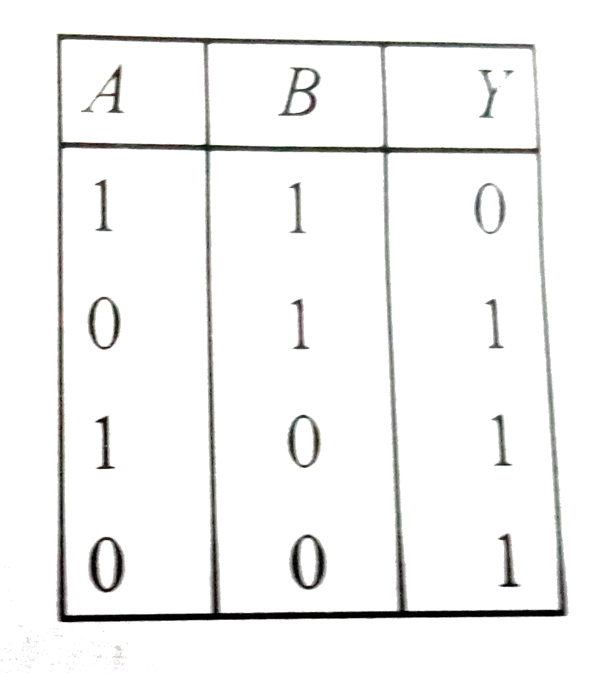
View SolutionWhich of the following truth tables corresponds to NAND gate ?
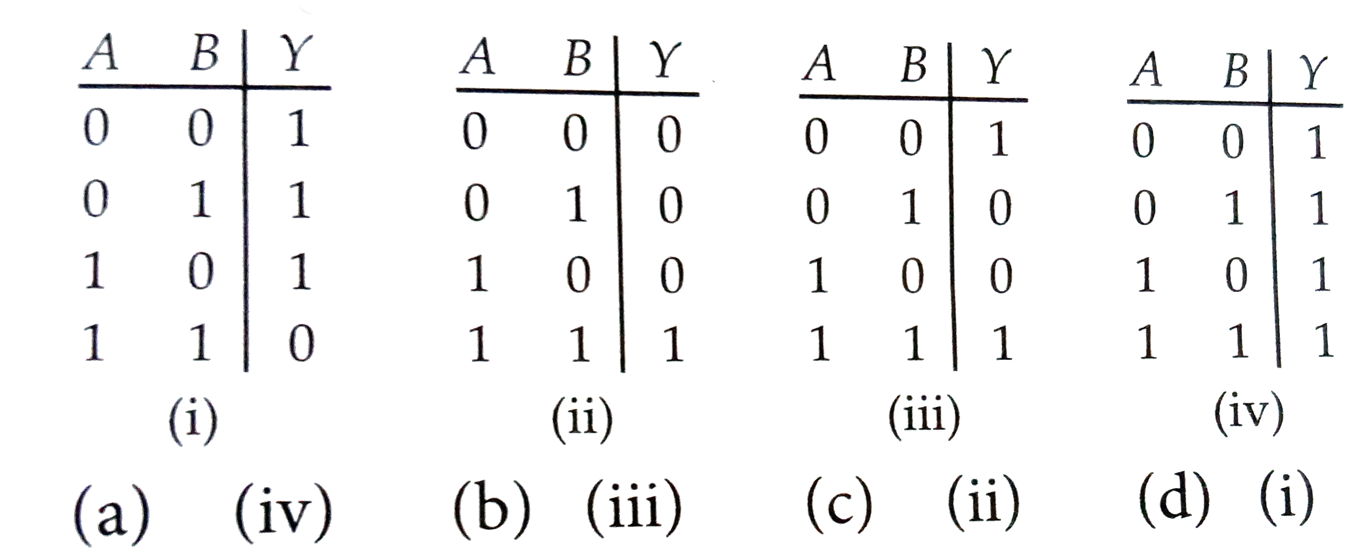
View SolutionThe decimal equivalent of the binary number `(11010.101)_(2)` is
View SolutionThe following figure shows a logic gate circuit with two inputs A and B and the output Y. The voltage waveforms of A,B and Y are as given :
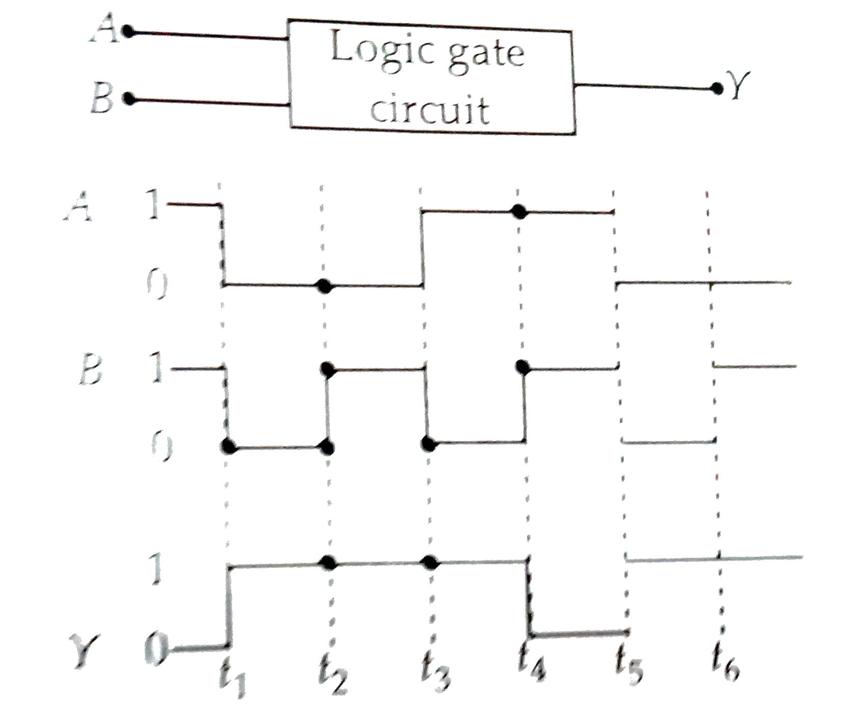
The logic gate is
View SolutionThe logic circuit shown below has the input waveforems 'A' and 'B' as shown. Pick out the correct output waveform
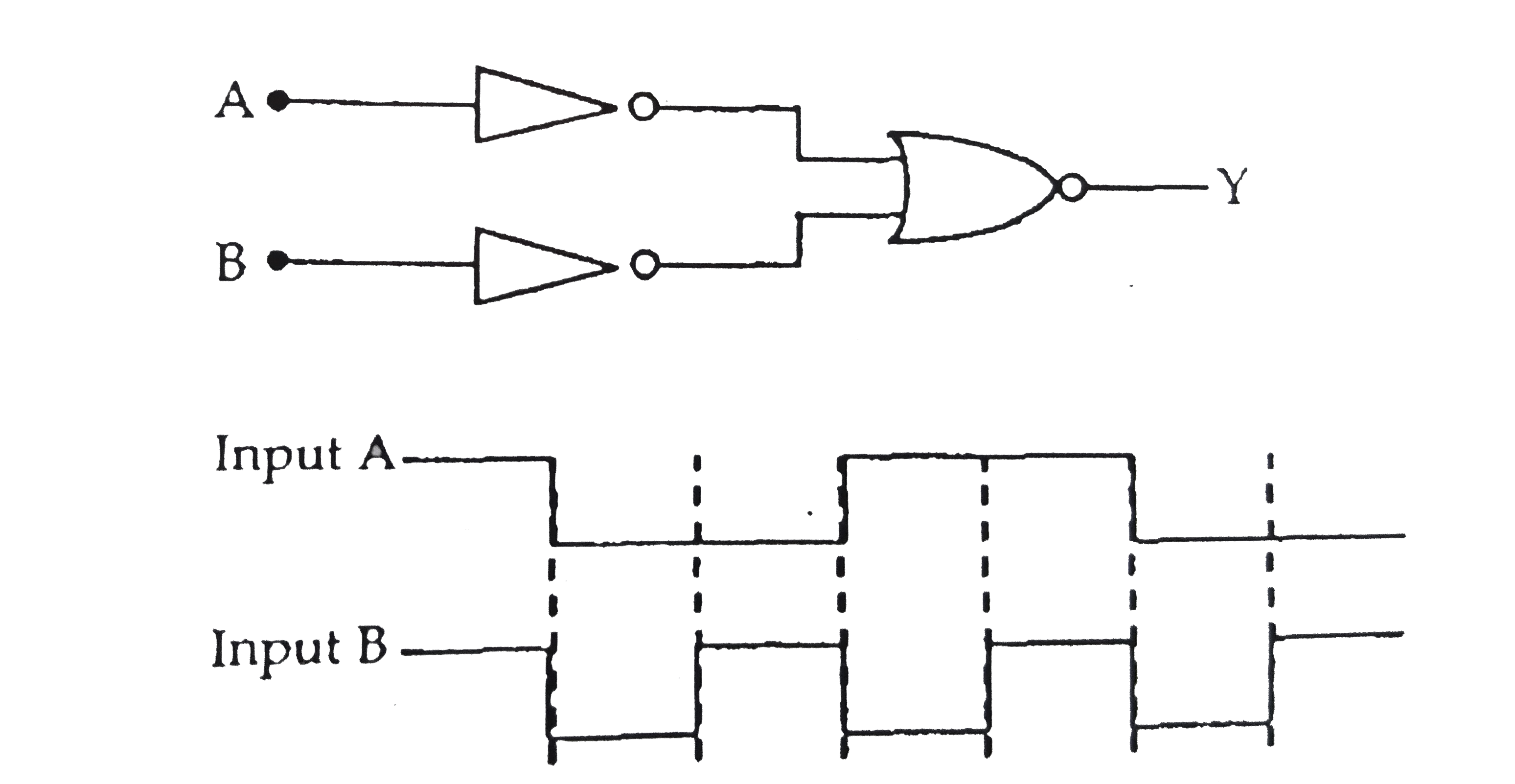
View Solution
MCQ questions and complete solutions for chapter SEMICONDUCTOR ELECTRONICS : MATERIALS , DEVICES AND SIMPLE CIRCUITS of MTG PHYSICS (ENGLISH) of Class 12
All Exercises from NCERT FINGERTIPS Class 12 PHYSICS SEMICONDUCTOR ELECTRONICS : MATERIALS , DEVICES AND SIMPLE CIRCUITS
- Application Of Junction Diode As A Rectifier
- ASSERTION & REASON
- Assertion And Reason
- Classification Of Metals, Conductors And Semiconductors
- Digital Electronics And Logic Gates
- Extrinsic Semiconductor
- Higher Order Thinking Skills
- HOTS
- Intrinsic Semiconductor
- Junction Transistor
- MCQ
- NCERT
- NCERT Exemplar
- P-N Junction
- Semiconductor Diode
- Special Purpose P-N Junction Diode