Complete Solutions to Junction Diode of chapter SEMICONDUCTOR ELECTRONICS of Class 12 book with complete answers and questions
| Class 12 | PHYSICS |
| Chapter | SEMICONDUCTOR ELECTRONICS |
| A2Z | Junction Diode |
| Number Of Questions | 57 |
| Academic Year | 2023-24 |
A semiconducting device is connected in a series circuit with a battery and a resistance.A current is found to pass through the circuit .If the polarity of the battery is reversed, the current drops to almost zero.The device may be
02:05View SolutionWhen a `PN` juction diode is forwards biased, energy is released at the juction due to the recombination of electrons and holes. This energy is in
01:42View SolutionBarrier potential of a `p-n` junction diode does not depend on
02:06View SolutionReverse bias applied to a junction diode
02:04View SolutionIn a `P-N` junction diode :
03:41View SolutionThe `PN` junction diode is used as
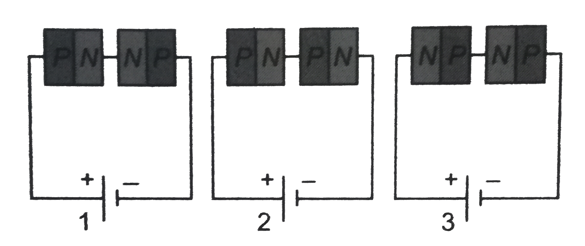
01:42View SolutionTwo `PN`-junction can be connected in series by three different methods as shown in the figure. If the potential difference in the junction is the same, then the correct connection will be
 01:48View Solution
On increases the reverse biase to a large value of in a `PN`- junction diode, current.
01:41View SolutionIn the forward biase arrangement of a `PN`-junction diode
03:32View SolutionIn a `PN` -junction diode
03:37View SolutionThe electrical circuit used to get smooth `dc` output from a rectifier circuit is called
02:07View Solution`PN`-junction diode works as a insulator, if connected
02:48View SolutionThe reverse biasing in a `PN` junction diode
03:45View SolutionThe electrical resistance of depletion layer is large because
02:30View SolutionIn junction diode, the holes lare due to
03:03View SolutionIn forward bias, the width of potential barrier in a `P-N` junction diode
03:05View SolutionIn a `P-N` junction diode is `P` region is heavily doped than `n` region then the depletion layer is
02:24View SolutionAvalanche breakdown is due to
03:03View SolutionZener breakdown in a semi-conductor diode occurs when
02:49View SolutionWhen `p- n` junction diode is forward baised then
01:07View SolutionFunction of rectifier is
01:42View SolutionWhen the `P` end of `P-N` junction is connected to the negative terminal of the battery and the `N` end to the
02:42View SolutionIf the two ends of a p-n junction are joined by a wire ,
02:28View SolutionA potential barrier of `0.50 V` exists across a `P-N` junction. If the depletion region is `5.0xx10^(-7)m`, wide the intensity of the electric field in this region is
01:35View SolutionIf no external voltage is applied across `P-N` junction, there would be
02:03View SolutionIn a `PN`-junction
01:32View SolutionOn adjusting the `P-N` junction diode in forward biased
02:27View SolutionIn the middle of the depletion layer of a reverse - biased `p - n ` junction , the
04:48View SolutionBarrier potential of a `p-n` junction diode does not depend on
02:06View SolutionA crystal diode is a
01:43View SolutionThe maximum effeciency of full wave rectifier is
03:03View SolutionSelect the correct statement
03:46View SolutionIn order to forward bias a `PN` junction, the negative terminal of battery is connected to
01:47View SolutionWhich one of the following statement is not correct?
02:50View SolutionTo make a `PN` junction conducting
03:33View SolutionZener breakdown takes place if
02:00View SolutionConsider the following statement `A` and `B` and identify the correct choice of the given answers
01:37View SolutionA device in which `P` and `N`-type semiconductors are used is more useful then a vacuum type because
View SolutionThe depletion layer in diode is `1 mum` wide and the knee potential is `0.6 V`, then the electric field in the depletion layer will be
01:06View SolutionIf a full wave reactifier circuit is operating from `50 Hz` mains, the fundamental frequency in the ripple will be
01:45View SolutionIn a p- n junction diode not connected to any circuit,
03:07View SolutionWhich of the following statement is not true ?
02:06View SolutionThe dominant mechanisms for motion of charge carriers in forward and reverse biased silicon `P-N` junction are
04:36View SolutionIn `P-N` junction, avalanche current flows in circuit when biassing is
03:30View SolutionThe depletion layer in `P-N` junction region is caused by
03:48View SolutionThe reason of current flow in `P-N` junction forward biase is
02:36View SolutionThe resistance of a revese biased `P-N` junction diode is about
01:56View SolutionNo biase is applied to a `P-N` junction, then the current
02:17View SolutionZener diode is used as
01:25View SolutionIn `P-N` junction, the barrier potential offerse resistance to
02:02View SolutionA semiconducting device is connected in a series circuit with a battery and a resistance.A current is found to pass through the circuit .If the polarity of the battery is reversed, the current drops to almost zero.The device may be
02:05View SolutionThe approximate ratio of resistance in the forward and reverse biase of the `PN-` junction diode is
01:55View SolutionIn a forward biased `PN`- junction diode, the potential barrier in the depletion region is of the from...
02:05View SolutionDifferent voltages are applied across a `P-N` junction and the currents are measured for each value. Which of the following graphs is obtained between voltage and current?
01:40View SolutionConsider the following statement `A` and `B` and identify the correct choice of the given answers
`A:` The width of the depletion layer in a `P-N` junction diode increases in forwards biase
`B:` In an intrinsic semiconductor the fermi energy level is exactely in the middle of the forbidden gap02:48View SolutionA `P`-type semiconductor has acceptor levels `57 meV` above the valence band. The maximum wavelength of light required to create a hole is (Planck's constant `h=6.6xx10^(-34)J-s`)
02:23View SolutionWhich one is forward biase?
01:41View Solution
Junction Diode questions and complete solutions for chapter SEMICONDUCTOR ELECTRONICS of A2Z PHYSICS (HINGLISH) of Class 12
