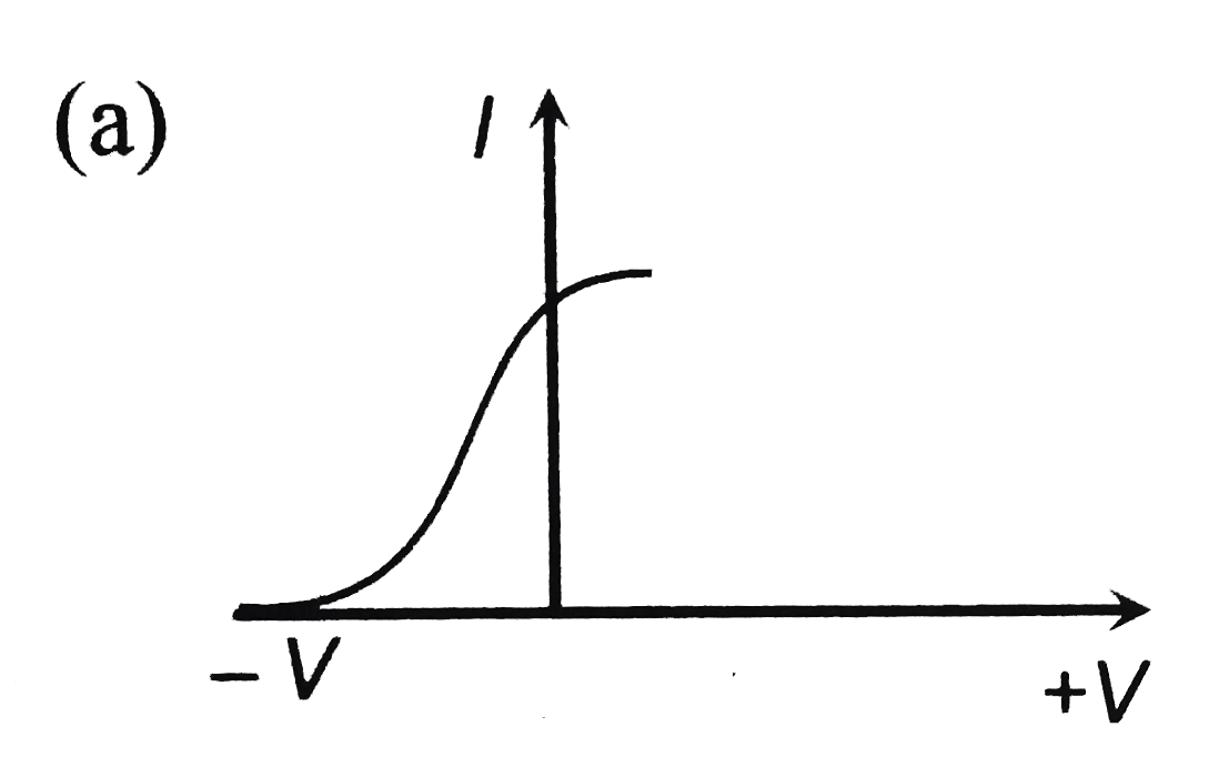
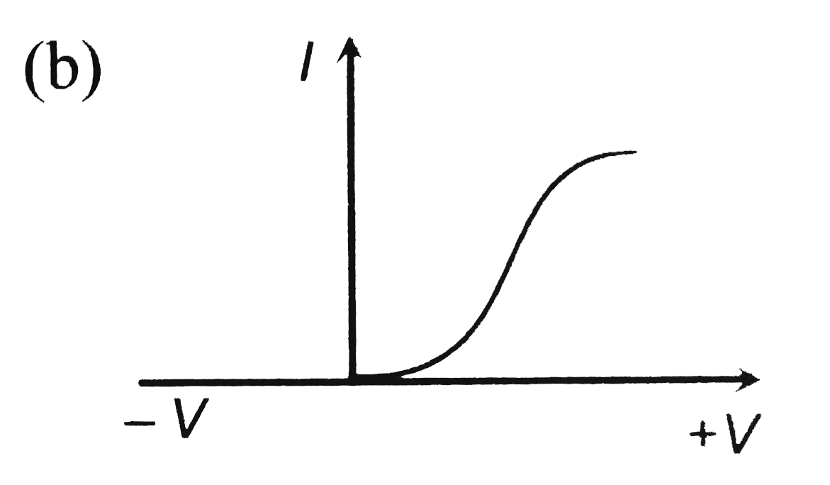
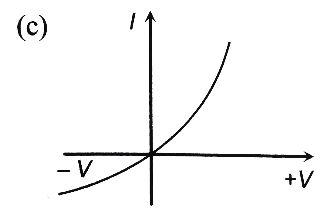
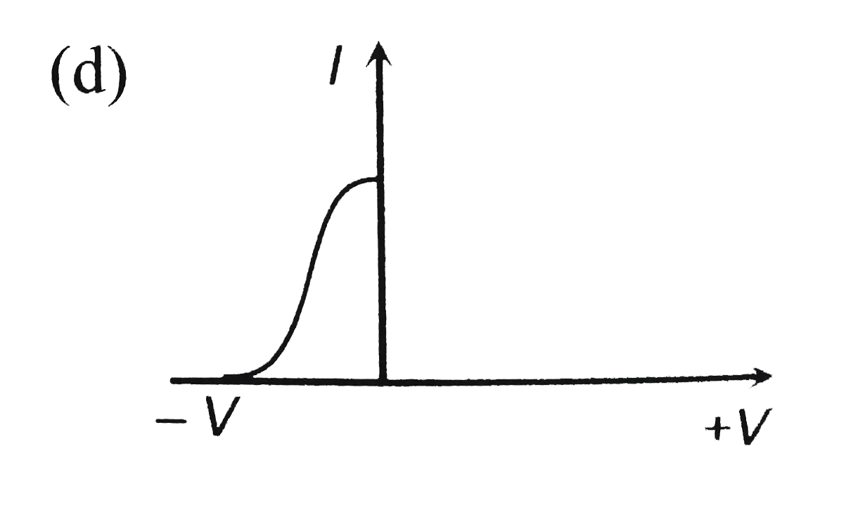
No biase is applied to a P−N junction, then the current
Is zero because the number of charge carriers flowing on both sides is same
Is zero because the charge carriers do not move
Is non zero
None of these
The correct Answer is:B
In unbiased condition of PN- junction, depletion region is generated which stops the movement of charge carriers.
Topper's Solved these Questions
- SEMICONDUCTOR ELECTRONICSBOOK - A2ZCHAPTER - SEMICONDUCTOR ELECTRONICSEXERCISE - Diode In Circuits
40 Videos
- SEMICONDUCTOR ELECTRONICSBOOK - A2ZCHAPTER - SEMICONDUCTOR ELECTRONICSEXERCISE - Junction Transistor
47 Videos
- SEMICONDUCTOR ELECTRONICSBOOK - A2ZCHAPTER - SEMICONDUCTOR ELECTRONICSEXERCISE - Classification Of Metals
64 Videos
- NUCLEAR PHYSICSBOOK - A2ZCHAPTER - NUCLEAR PHYSICSEXERCISE - Section D - Chapter End Test
29 Videos
- SOURCE AND EFFECT OF MAGNETIC FIELDBOOK - A2ZCHAPTER - SOURCE AND EFFECT OF MAGNETIC FIELDEXERCISE - Section D - Chapter End Test
30 Videos
Similar Questions
Explain with the help of a diagram, how depletion region and potential barrier are formed in a junction diode.
If a small voltage is applied to a p-n junction diode how will the barrier potential be affected when it is (i) forward biased and (ii) reverse biased?
View SolutionName the type of biasing of a p-n junction diode so that the junction offers very high resistance.
View Solution
Knowledge Check
No bias is applied to a P-N junction, then the current-
AIs zero because the number of charge carriers flowing on both sides is sameBis zero because the charge carriers do not moveCIs non-zeroDNone of theseDifferent voltages are applied across a P−N junction and the currents are measured for each value. Which of the following graphs is obtained between voltage and current?
A B
B C
C D
D
When a forward bias is applied to a p-n junction, it
Araises the potential barrier.Breduces the majority carrier current to zero.Clowers the potential barrier.Dnone of the above.
When a forward bias is applied to a p -n junction. It
View SolutionA potential difference is applied across (i) an issulator at 0 k (ii) a semiconductor at 0 k (iii) a metal at 0 k (iv) a reverse biased p-n junction diode at 300 k then the current passing through
View SolutionOn increases the reverse biase to a large value of in a PN- junction diode, current.
View SolutionAssertion:The dominant mechanism for motion of charge carriers in forward and reverse biased silicon P−N junction are drift in both forward and reverse biase.
Reason: In reverse biasing, no current flow through the junction.
View SolutionAssertion : The dominant mechanism for motion of charge carreis in forward and reverse biased silicon P-N junction are drit in both forward and reverse bias.
Reaon : In reverse biasing, no current flow through the junction.
View Solution
