Complete Solutions to Section B - Assertion Reasoning of chapter SEMICONDUCTOR ELECTRONICS of Class 12 book with complete answers and questions
| Class 12 | PHYSICS |
| Chapter | SEMICONDUCTOR ELECTRONICS |
| A2Z | Section B - Assertion Reasoning |
| Number Of Questions | 22 |
| Academic Year | 2023-24 |
Assertion: If the temperature of a semiconductor is increased then its resistance decreases.
Reason: The energy gap between conduction band and valence band is very small02:59View SolutionAssertion: Electron has higher mobility than hole in a semiconductor.
Reason: Mass of electron is less than the mass of hole.01:43View SolutionAssertion : An `N`-type semiconductor has a large number of electrons but still it is electrically neutral.
Reason: An `N`-type semiconductor is obtained by doping an intrinsic semiconductor with a pentavelent impurity.03:58View SolutionAssertion : The crystalline solids have a sharp melting point.
Reason: All the bonds between the atoms or molecules fo a crystalline solids are equally strong, that they get broken at the same temperature.01:47View SolutionAssertion: Silicon is preferred over germanium for making semiconductor devices.
Reason: The energy gap for germanium is more than the energy gap of silicon.01:58View SolutionAssertion: Two `P-N` junction diodes placed back to back, will work as a `NPN` transistor.
Reason: The `P-N` junction of two `PN` junction diodes back to back will form the base of `NPN` transistor.03:47View SolutionAssertion : In transistor common emitter mode as an amplifier is prefered over common base mode.
Reason: In common emitter mode the input signal is connected in series with the voltage applied to the base emitter function.03:13View SolutionAssertion:The dominant mechanism for motion of charge carriers in forward and reverse biased silicon `P-N` junction are drift in both forward and reverse biase.
Reason: In reverse biasing, no current flow through the junction.04:31View SolutionAssertion: A transistor is a voltage-operating device.
Reason: Base current is greater than the collector current.02:25View SolutionAssertion: `NAND` or `NOR` gates are called digital building blocks.
Reason: The repeated use of `NAND` (or `NOR`) gates can produce all the basic or complicated gates.03:17View SolutionAssertion: At `0K` germanium is a superconductor.
`Reason: At `0K` germanium offers zero resistance.02:17View SolutionAssertion: Base in transistor is made very thin as compared to collector and emitter regions.
Reason: Due to thin base power gain and voltage gain is obtained by a transistor.02:55View SolutionAssertion: The current gain in common base circuit is always less than one.
Reason: At constant collector votalge the change in collector current is more than the change in emitter current.01:58View SolutionAssertion: `V-i` charcteristic of `P-N` junction diode is same as that of any other conductor.
Reason: `P-N` junction diode behaves as conductor at room temperature.02:23View SolutionAssertion: Zener diode works on a principle of of breakdown voltage.
Reason: Current increases suddenly after breakdown voltage.01:20View SolutionAssertion: `NOT` gate is also called inverter circuit.
Reason: `NOT` gate inverts the input order.01:23View SolutionAssertion: In vacuum tubes (vales), vacuum is necessary for the movement of electrons between electrods otherwise electrons collide with air and loss their energy.
Reason: In semiconductor devices, external heating or vacuum is not required.01:23View SolutionAssertion: The following circuit represents `'OR'` gate

Reason: For the above circuit `Y=bar(X)=bar(bar(A+B))=A+B`01:23View SolutionAssertion: A `P-N` photodiode is made from a semiconductor for which `E_(g)=2.8 eV`. This photo diode will not detect the wavelength of `6000 nm`.
Reason: A `PN` photodiode detect wavelength `lambda` if `(hc)/(lambda)gtE_(g)`.03:20View SolutionAssertion: When `PN`-junction is forward biased then motion of charge carriers at junction is due to diffusion. In reverse biasing. The cause of motion of charge is drifting.
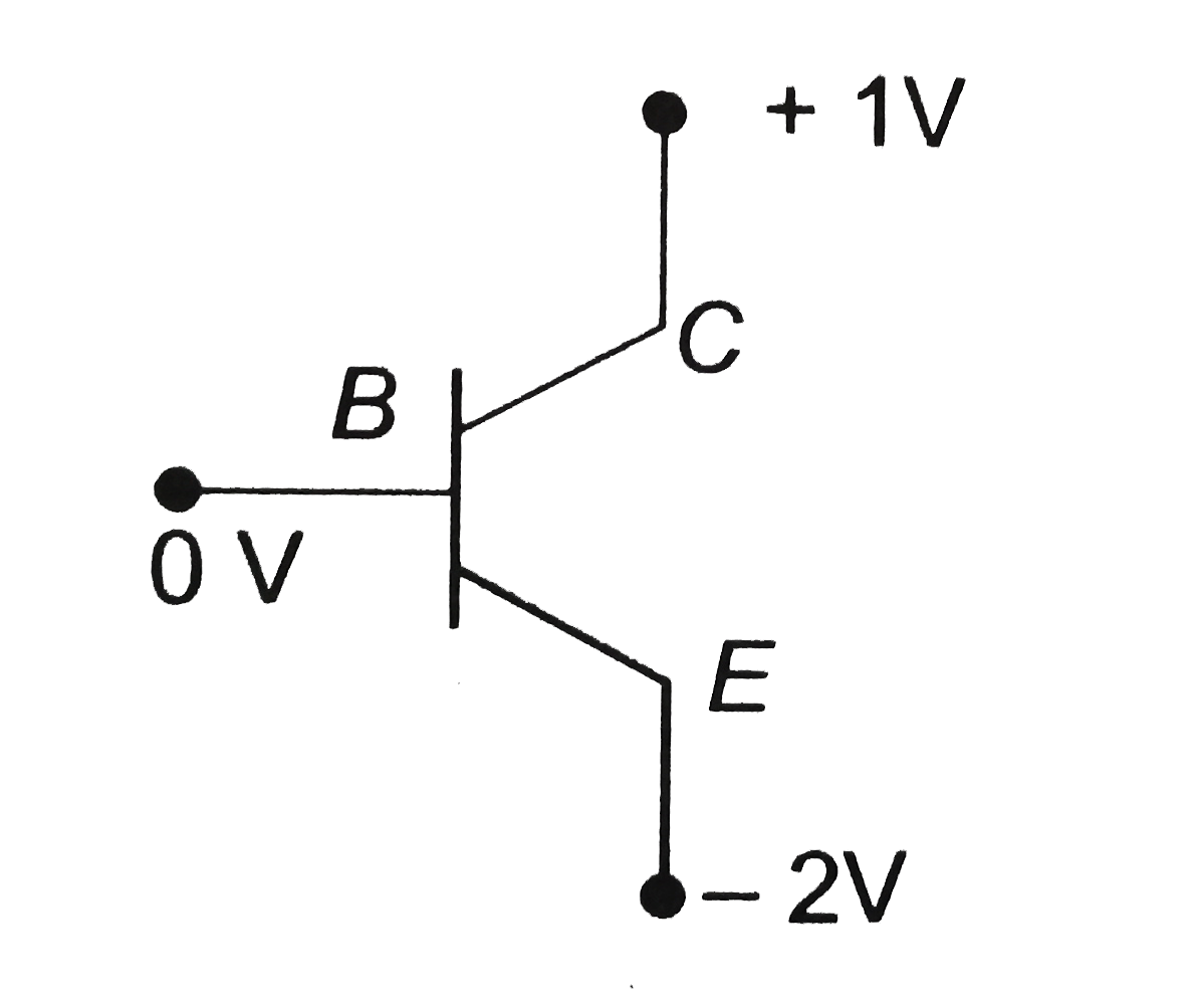
Reason: In the following circuit emitter is reverse biased and collector is forward biased.
 05:07View Solution
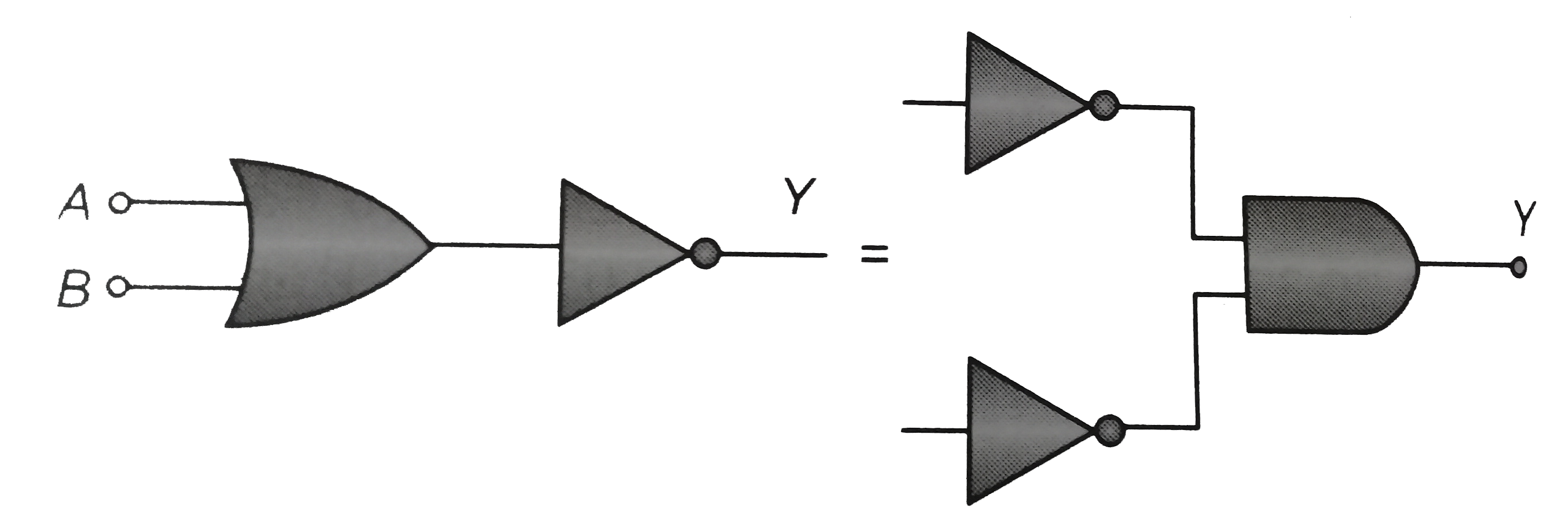
Assertion: De Morgan's theoram `bar(A+B)=bar(A).bar(B)` may be explained by the following circuit.

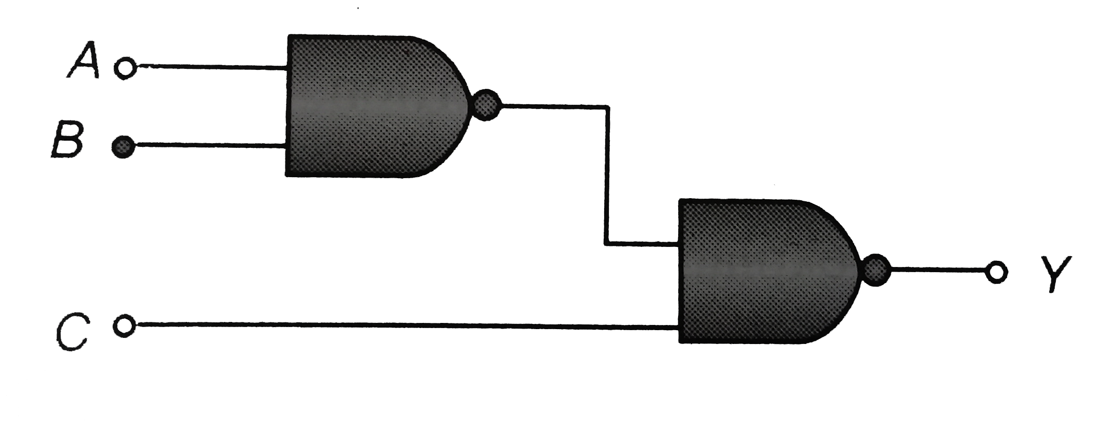
Reason: In the following circuit, for output, inputs `ABC` are `101`.
 03:53View Solution
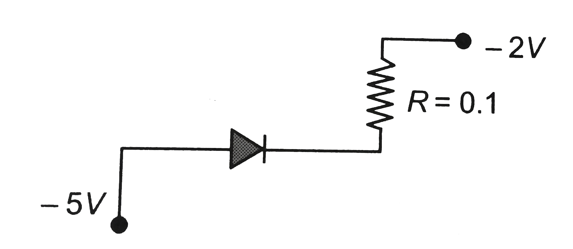
Assertion: In the following circuit the potential drop across the resistance is zero.

Reason: The given resistance has low value.02:09View Solution
Section B - Assertion Reasoning questions and complete solutions for chapter SEMICONDUCTOR ELECTRONICS of A2Z PHYSICS (HINGLISH) of Class 12
