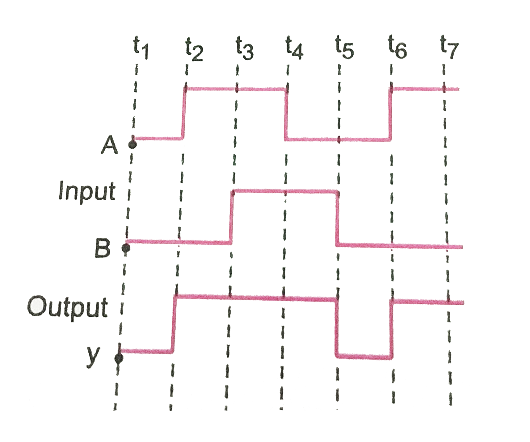
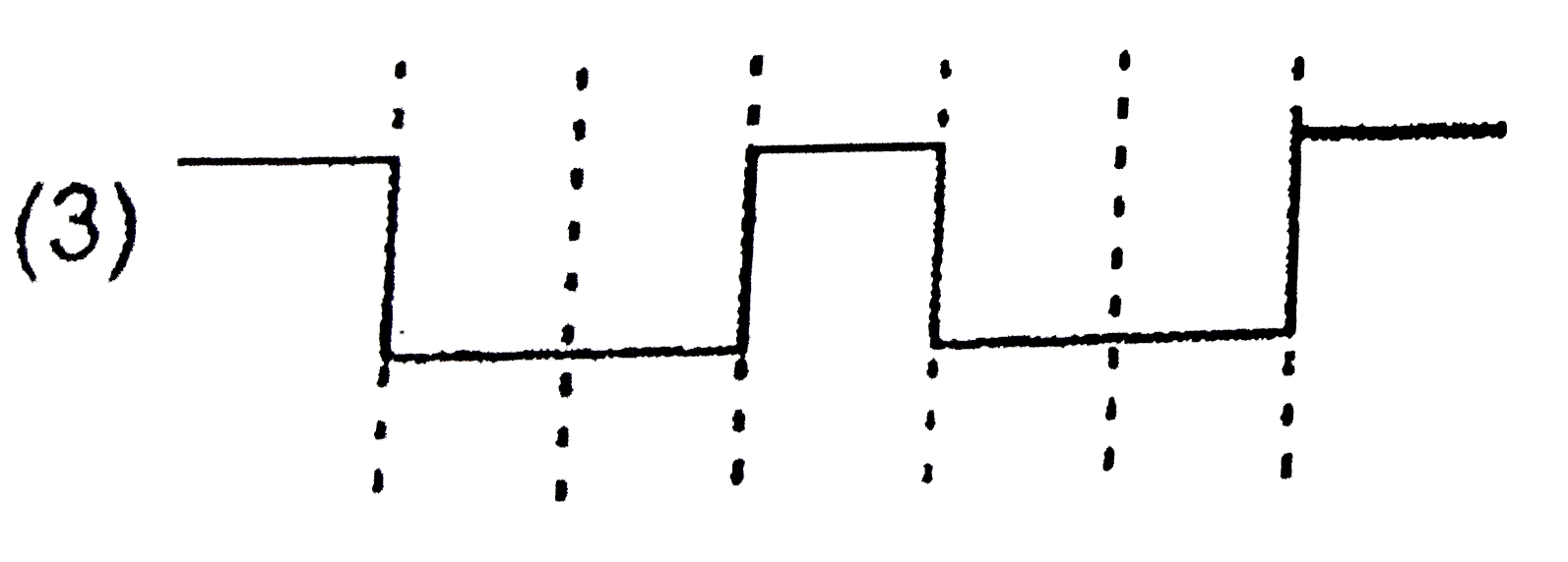
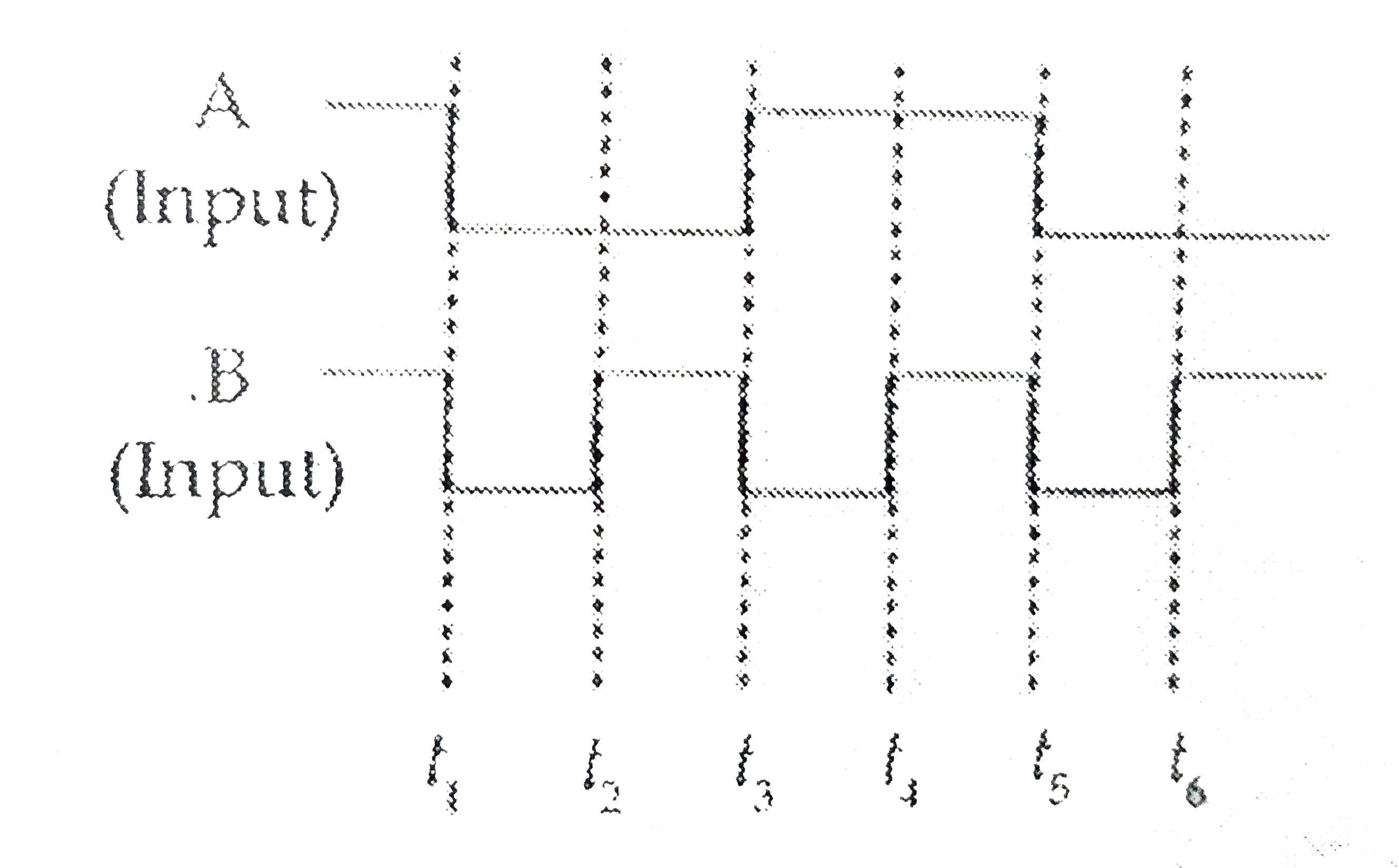
The Fig shown input waveforms A and B to a logic gate. Draw the output waveform for an OR gate. Write the truth table for this logic gate and draw its logic symbol.
A

B

C
D

Video Solution
Text Solution
The correct Answer is:D
If lattice constant of semiconductor is decreased, then EC and EV decrease but Eg increase.
|
Topper's Solved these Questions
- SEMICONDUCTORSBook:RESONANCE ENGLISHChapter:SEMICONDUCTORSExercise:Exercise 2
Explore 16 Videos
- REVISION DPPBook:RESONANCE ENGLISHChapter:REVISION DPPExercise:All Questions
Explore 463 Videos
- SIMPLE HARMONIC MOTION Book:RESONANCE ENGLISHChapter:SIMPLE HARMONIC MOTION Exercise:Advanced Level Problems
Explore 13 Videos
Similar Questions
Knowledge Check

The truth table of the logic circuit shown-A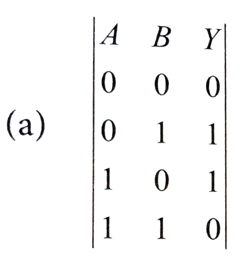 B
B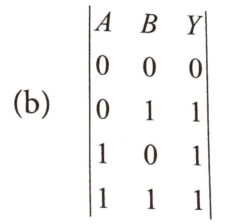 C
C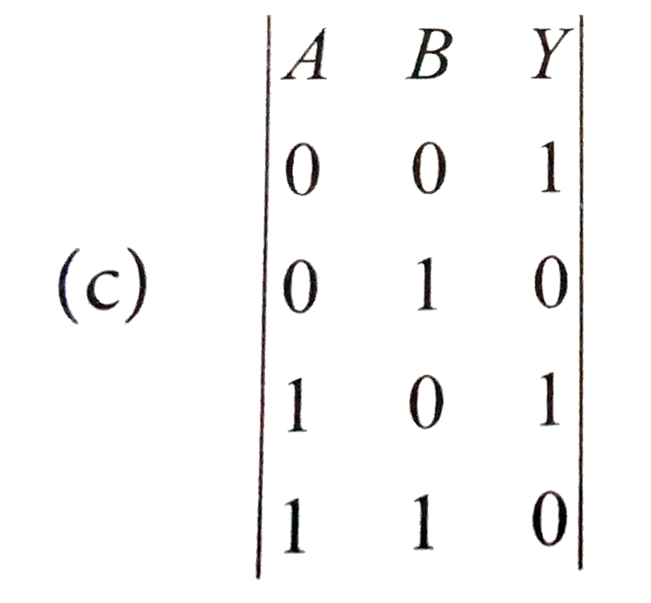 D
D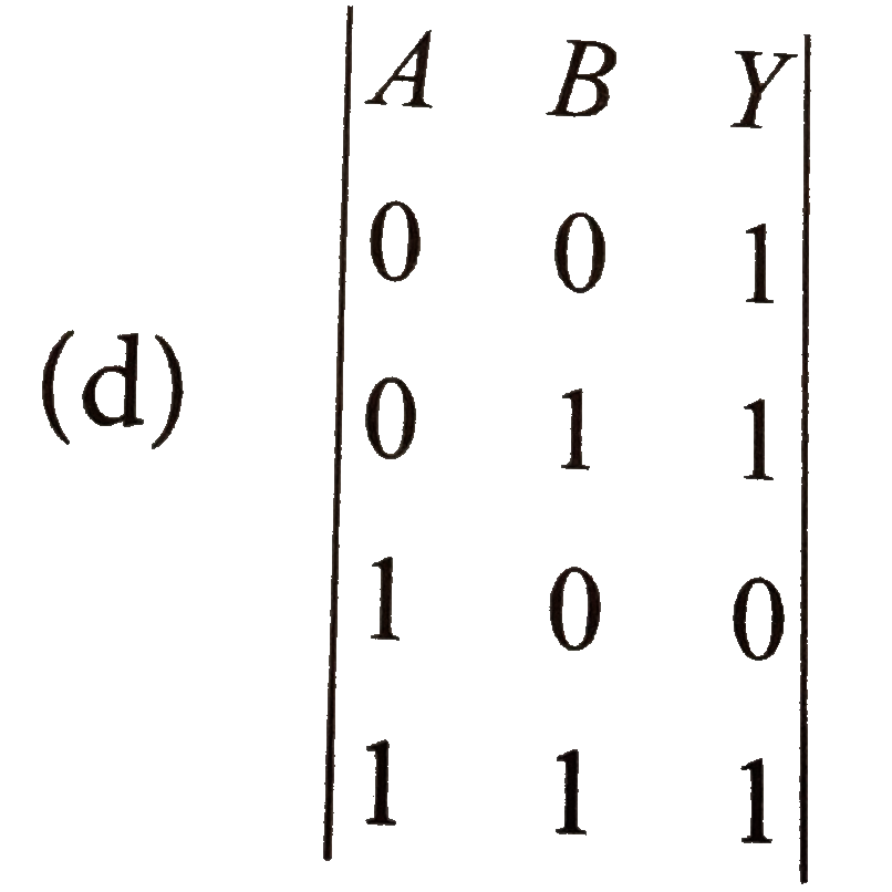
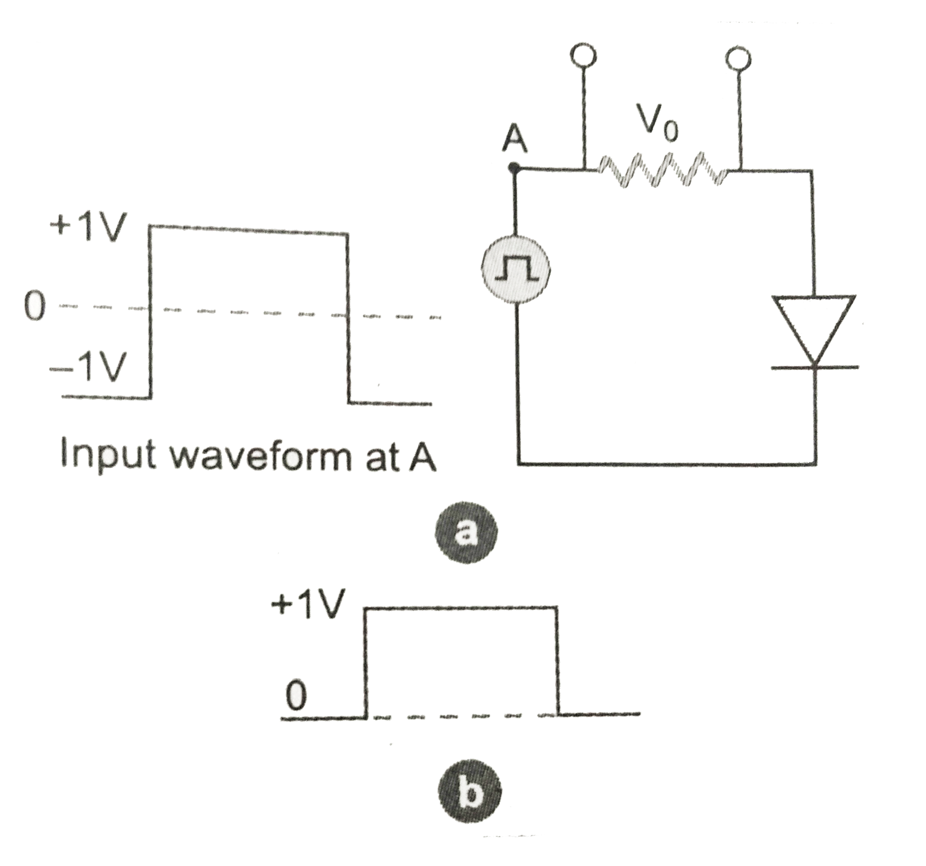
Draw the output waveform across the resistor (Fig.)
View Solution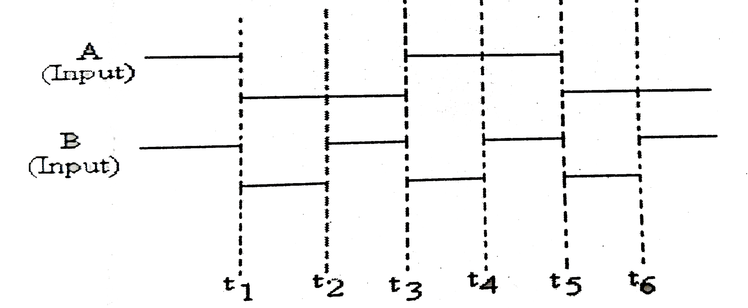
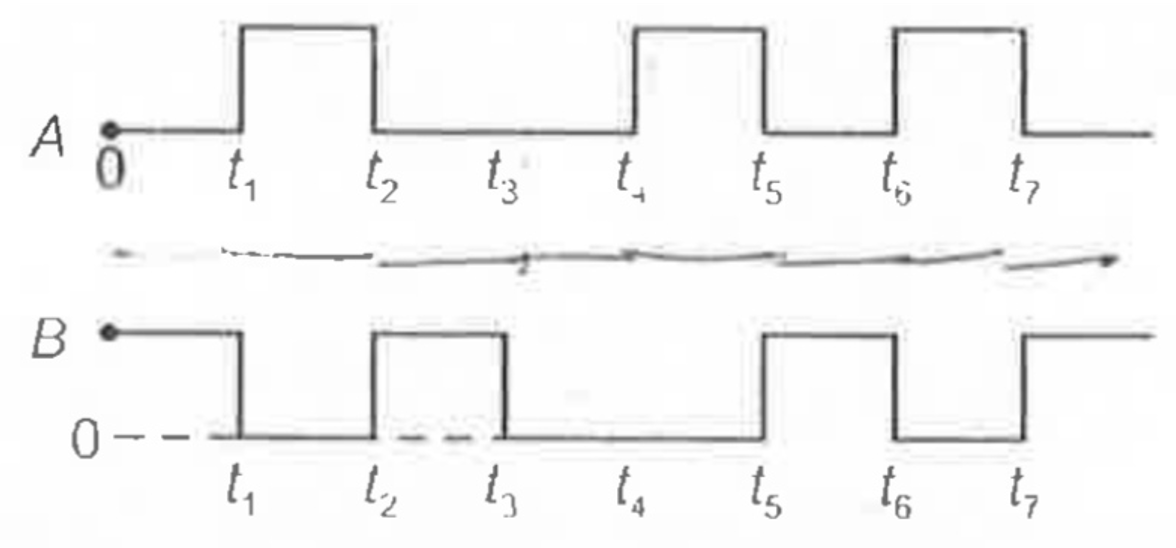
The give inputs A, B are fed to a 2-input NAND gate. Draw the output wave form of the gate.
View SolutionThe given input A, B are fed to a 2-input NAND gate. Draw the output wave form of the gate
View SolutionWhat is the symbol of a NOR gate? Write its truth table.
View SolutionWhat is a NAND gate ? Write its truth table.
View SolutionThe output waveform of AND gate for the following input waveforms is
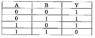
View SolutionIdentify the logic gate whose truth table is given below and draw its symbol :
View Solution


 .
.