Draw the truth table of a NOR gate.
To draw the truth table for a NOR gate, we need to understand the behavior of the gate based on its inputs. A NOR gate is a digital logic gate that outputs true or 1 only when both inputs are false or 0.
1. Identify Inputs and Output:
- The NOR gate has two inputs, which we will denote as A and B.
- The output will be denoted as Y.
2. Write Down Possible Input Combinations:
- Since there are two inputs (A and B), we can have the following combinations:
- A = 0, B = 0
- A = 0, B = 1
- A = 1, B = 0
- A = 1, B = 1
3. Determine Output for Each Combination:
- For each combination of inputs, we will determine the output Y based on the NOR operation, which is defined as:
- Y = (A NOR B) = NOT (A OR B)
- Now we will evaluate the output for each combination:
- When A = 0, B = 0:
- A OR B = 0 OR 0 = 0
- Y = NOT(0) = 1
- When A = 0, B = 1:
- A OR B = 0 OR 1 = 1
- Y = NOT(1) = 0
- When A = 1, B = 0:
- A OR B = 1 OR 0 = 1
- Y = NOT(1) = 0
- When A = 1, B = 1:
- A OR B = 1 OR 1 = 1
- Y = NOT(1) = 0
4. Construct the Truth Table:
- Now we can summarize the results in a truth table format:
| A | B | Y (A NOR B) |
|---|---|-------------|
| 0 | 0 | 1 |
| 0 | 1 | 0 |
| 1 | 0 | 0 |
| 1 | 1 | 0 |
Final Truth Table:
|A|B|Y(ANORB)|⊢−⊢−⊢−−−−−−−−−−−||0|0|1||0|1|0||1|0|0||1|1|0∣
- The NOR gate has two inputs, which we will denote as A and B.
- The output will be denoted as Y.
- Since there are two inputs (A and B), we can have the following combinations:
- A = 0, B = 0
- A = 0, B = 1
- A = 1, B = 0
- A = 1, B = 1
- For each combination of inputs, we will determine the output Y based on the NOR operation, which is defined as:
- Y = (A NOR B) = NOT (A OR B)
- Now we will evaluate the output for each combination:
- When A = 0, B = 0:
- A OR B = 0 OR 0 = 0
- Y = NOT(0) = 1
- When A = 0, B = 1:
- A OR B = 0 OR 1 = 1
- Y = NOT(1) = 0
- When A = 1, B = 0:
- A OR B = 1 OR 0 = 1
- Y = NOT(1) = 0
- When A = 1, B = 1:
- A OR B = 1 OR 1 = 1
- Y = NOT(1) = 0
- Now we can summarize the results in a truth table format:
|---|---|-------------|
| 0 | 0 | 1 |
| 0 | 1 | 0 |
| 1 | 0 | 0 |
| 1 | 1 | 0 |
|A|B|Y(ANORB)|⊢−⊢−⊢−−−−−−−−−−−||0|0|1||0|1|0||1|0|0||1|1|0∣
Similar Questions
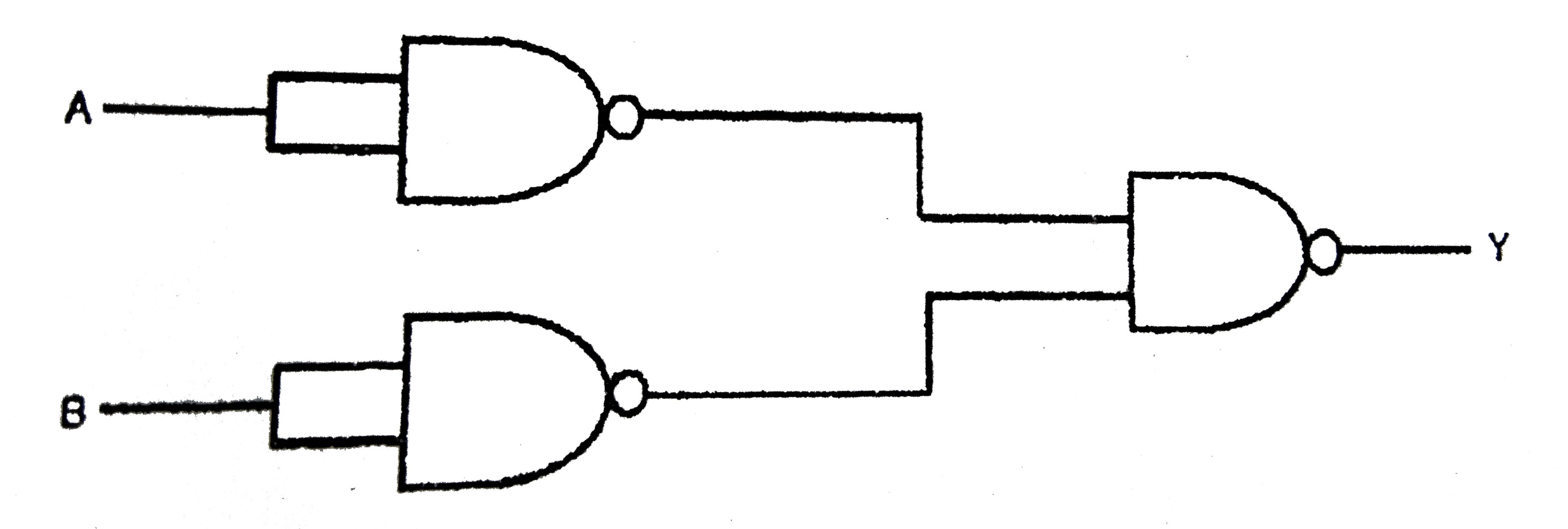
Write the truth table for a NAND gate as given in Fig.9. Hence identify the exact logic operation carried out by this circuit.
 View Solution

(a) Draw the circuit diagram of reversed bias p-n junction.
(b). Draw the output wavefrom across diode in given circuit.
(c). Draw the truth table for the given logic gate.View SolutionGive the truth table of ~p∨q
View Solution
Draw the truth table for the logic gate arrangement shown in the figure.View SolutionShow how you will obtain an AND gate using only NOR gates. Draw the truth table for this arrangement of gates.
View SolutionGive Boolean expression and Truth table for NOR gate.
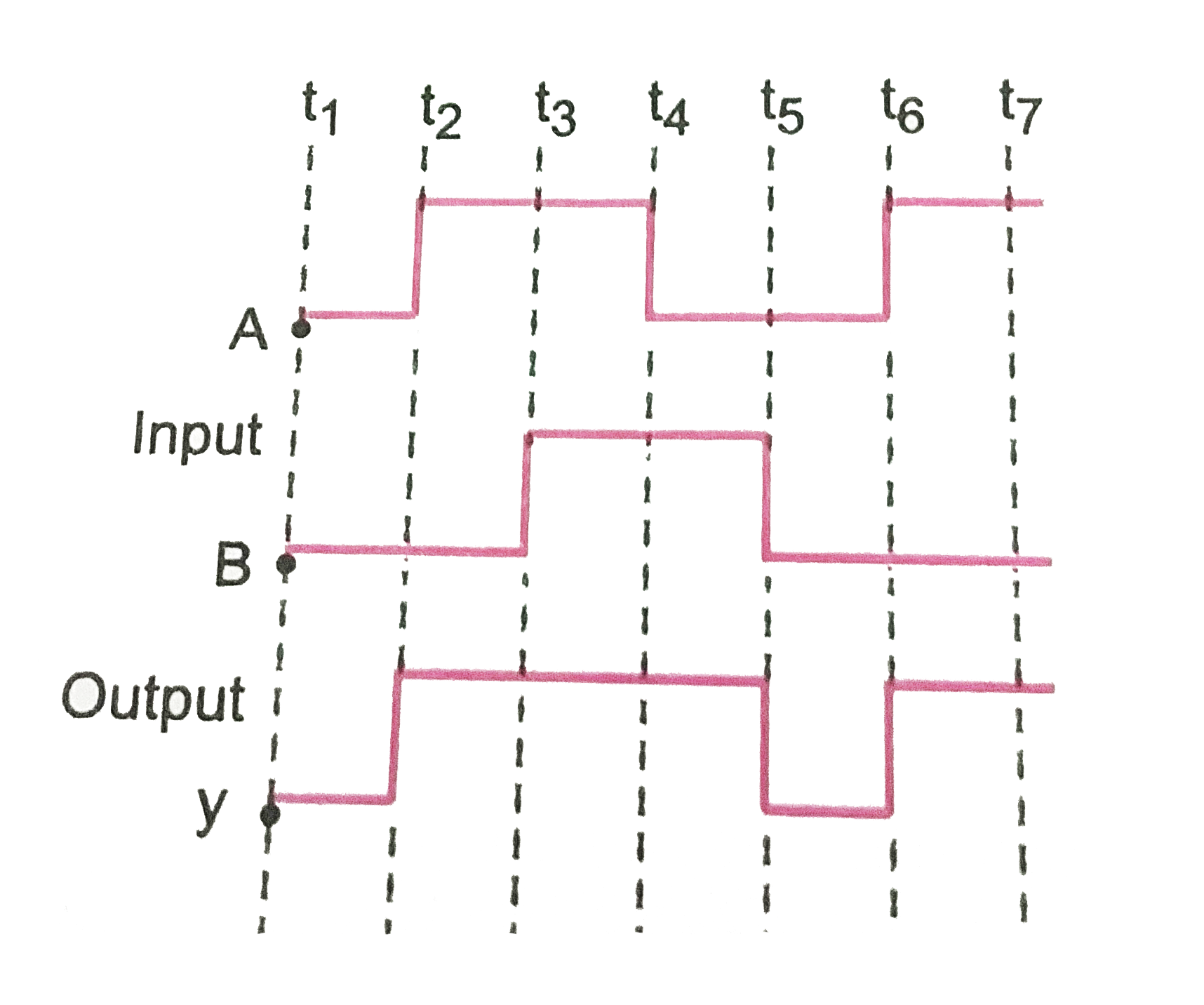
View SolutionThe Fig shown input waveforms A and B to a logic gate. Draw the output waveform for an OR gate. Write the truth table for this logic gate and draw its logic symbol.
 View Solution
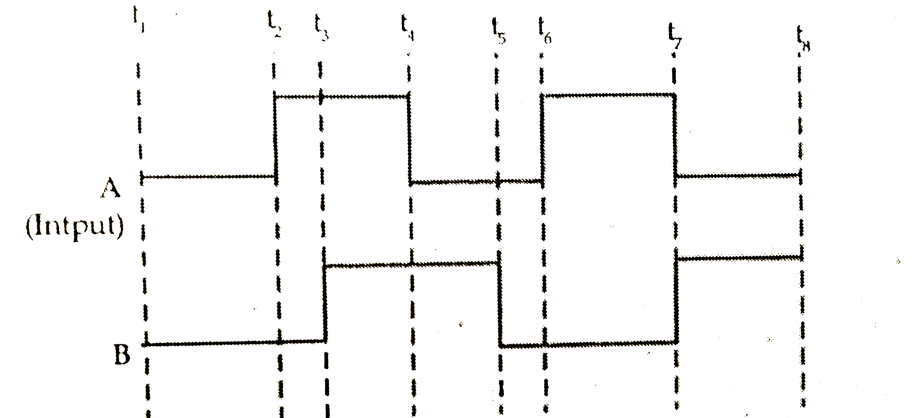
The figure shows the input weveforms A and B for 'AND' gate Draw the output waveform and write the truth table for this logic gate
 . View Solution
Construct the truth table for p∧q.
View SolutionWrite the truth table of the following circuit. Name the gate represented by this circuit.
 View Solution
