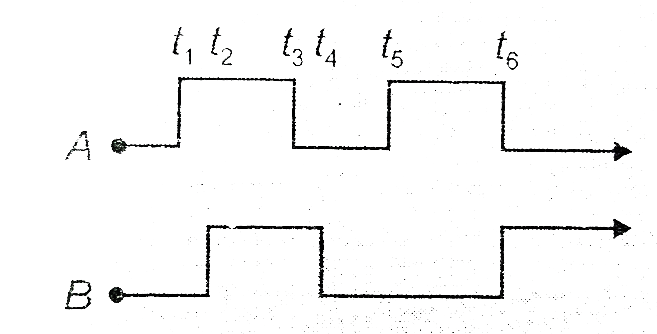
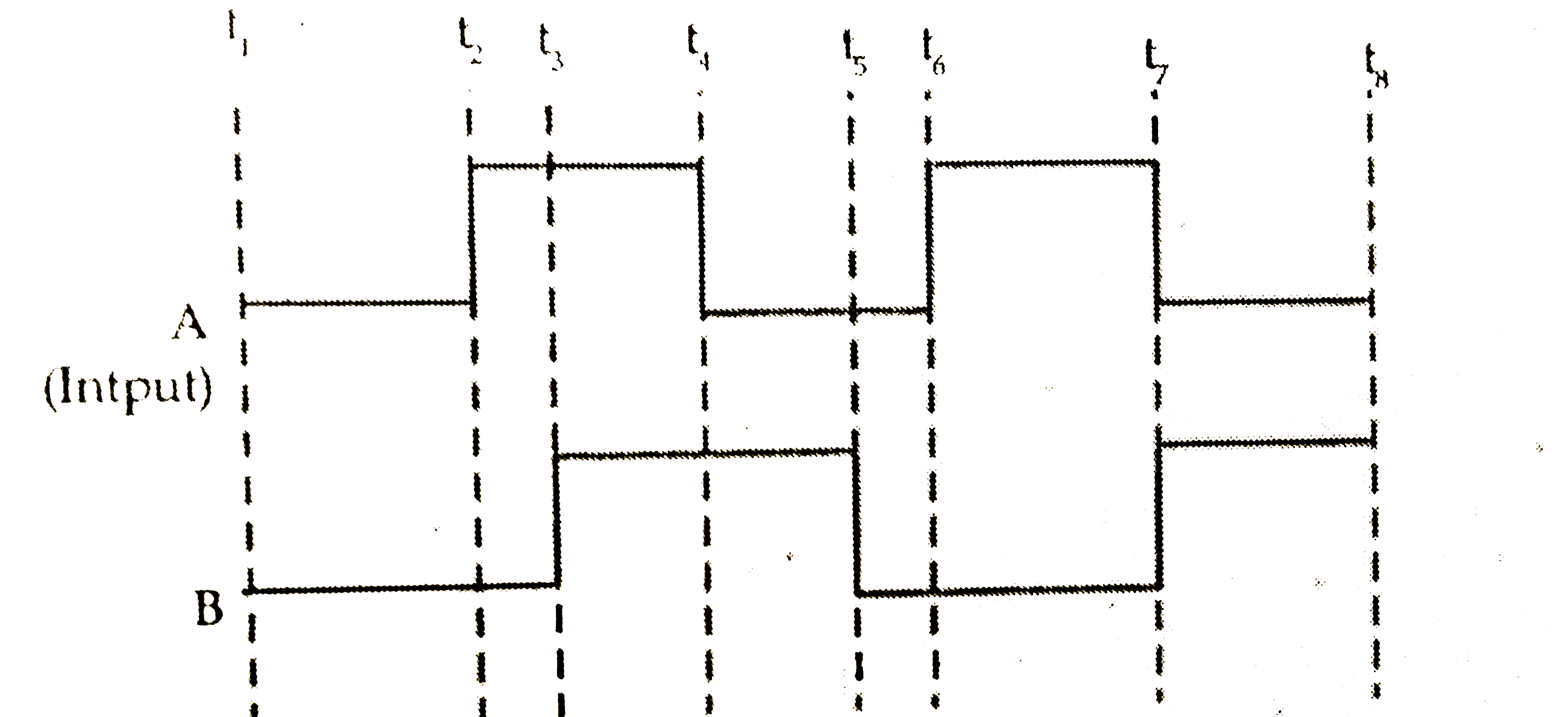
Sketch the output waveform obtained from AND gate for the following inputs A and B.
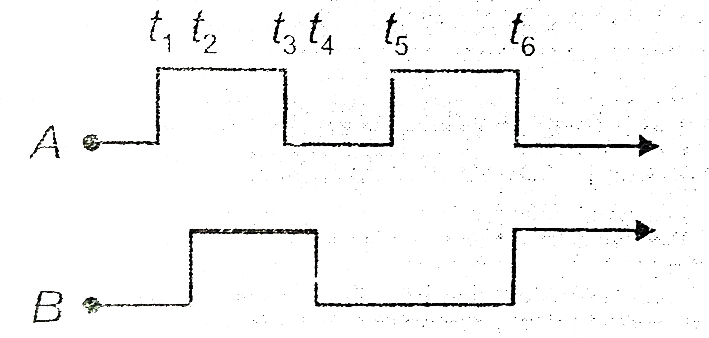
(##AAK_P7_NEET_PHY_SP7_C29_E01_026_S01.png" width="80%">
Topper's Solved these Questions
- SEMICONDUCTOR ELECTRONICS (MATERIAL, DEVICES AND SIMPLE CIRUITS )BOOK - AAKASH INSTITUTE ENGLISHCHAPTER - SEMICONDUCTOR ELECTRONICS (MATERIAL, DEVICES AND SIMPLE CIRUITS )EXERCISE - EXERCISE
20 Videos
- SEMICONDUCTOR ELECTRONICS (MATERIAL, DEVICES AND SIMPLE CIRUITS )BOOK - AAKASH INSTITUTE ENGLISHCHAPTER - SEMICONDUCTOR ELECTRONICS (MATERIAL, DEVICES AND SIMPLE CIRUITS )EXERCISE - Assignment section -A (Objective Type Question)
43 Videos
- SEMICONDUCTOR ELECTRONICS (MATERIAL, DEVICES AND SIMPLE CIRUITS )BOOK - AAKASH INSTITUTE ENGLISHCHAPTER - SEMICONDUCTOR ELECTRONICS (MATERIAL, DEVICES AND SIMPLE CIRUITS )EXERCISE - Assignment SECTION - D (Assertion & reason type Question)
10 Videos
- RAY OPTICS AND OPTICAL INSTRUMENTSBOOK - AAKASH INSTITUTE ENGLISHCHAPTER - RAY OPTICS AND OPTICAL INSTRUMENTSEXERCISE - ASSIGNMENT (SECTION - D)
16 Videos
- SEMICONDUCTOR ELECTRONICS: MATERIALS, DEVICES AND SIMPLE CIRCUITSBOOK - AAKASH INSTITUTE ENGLISHCHAPTER - SEMICONDUCTOR ELECTRONICS: MATERIALS, DEVICES AND SIMPLE CIRCUITSEXERCISE - Assignment (Section-D (Assertion and reason))
5 Videos
Similar Questions
Sketch the output waveform Y from a NAND gate having following inputs A and B
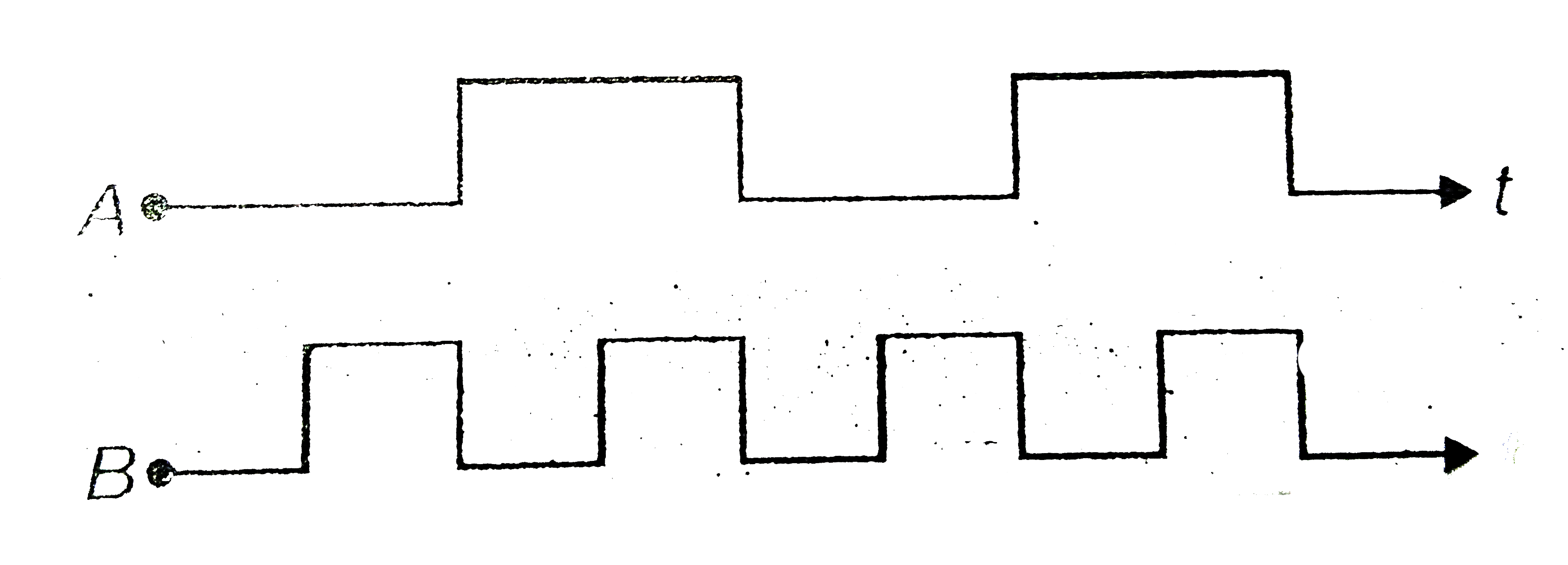
View SolutionThe output waveform of AND gate for the following input waveforms is
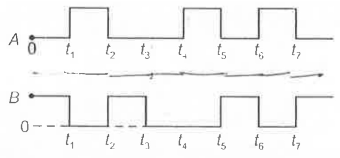
View Solutionshow the output waveform of AND gate for the following input waveforms of A and B.

View SolutionSketch the output wavefrom Y from a NAND gate having following inputs A and B
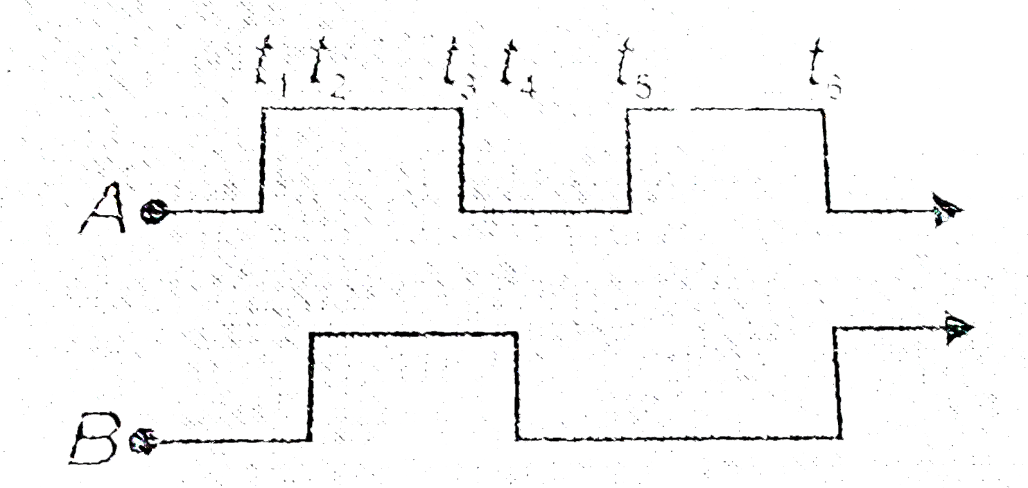
View SolutionShow the output waveform of OR gate for the following input waveforms of A and B

View SolutionShow the output waveform of OR gate for the following input waveforms of A and B
View Solution(i) Sketch the output waveform from an AND gate for the inputs A and B shown in the figure.
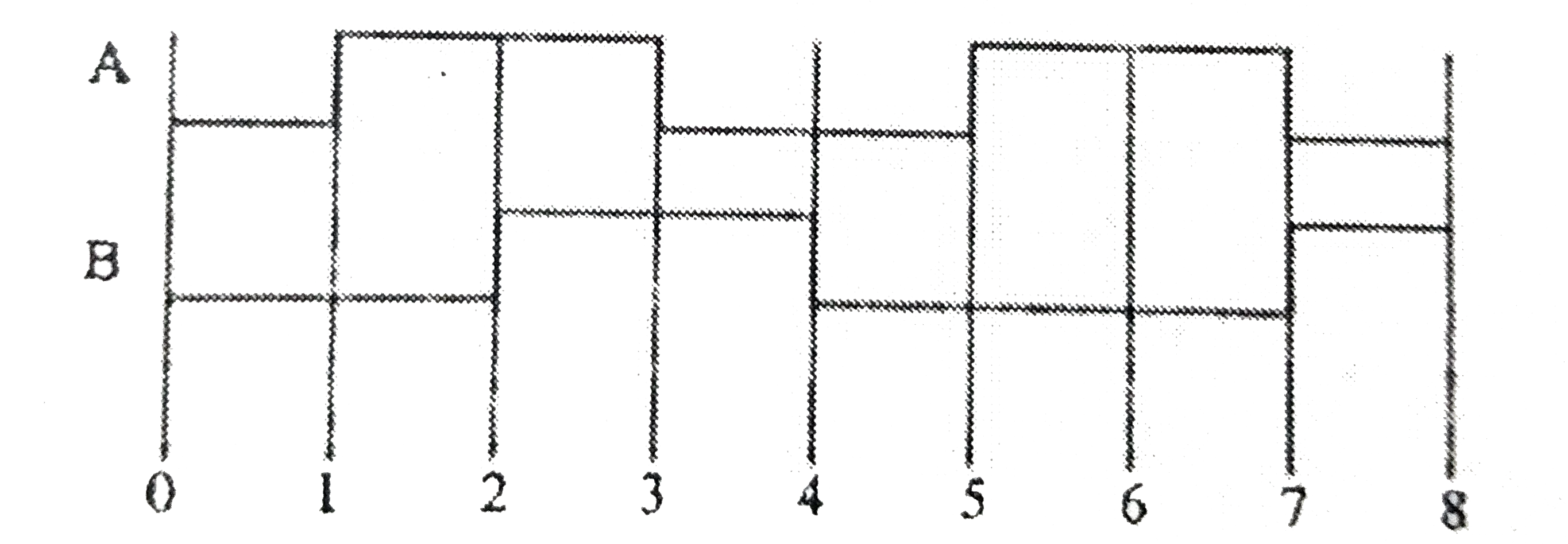
(ii) If the output of the above AND gate is fed to a NOT gate, name the gate of the combination so formed.
View Solution(a) Draw the circuit diagram of a full wave rectifier using p-n junction diole. Explain its working and show the output, input waveforms.
(b) Show the output waveforms (Y) for the following inputs A and B of (i) OR gate (ii) NAND gate :
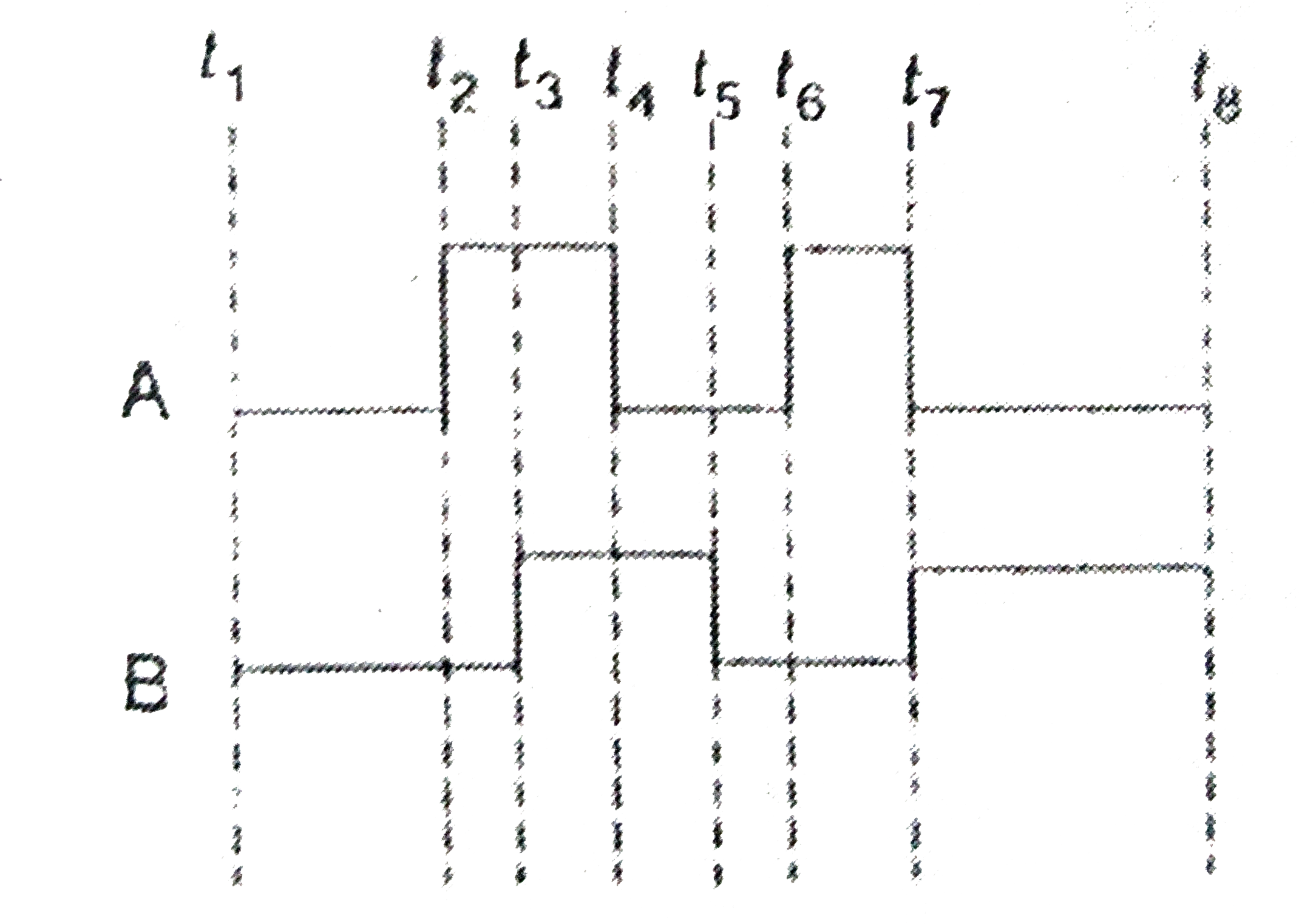
View SolutionDraw the output waveform across the resistor (Fig.)
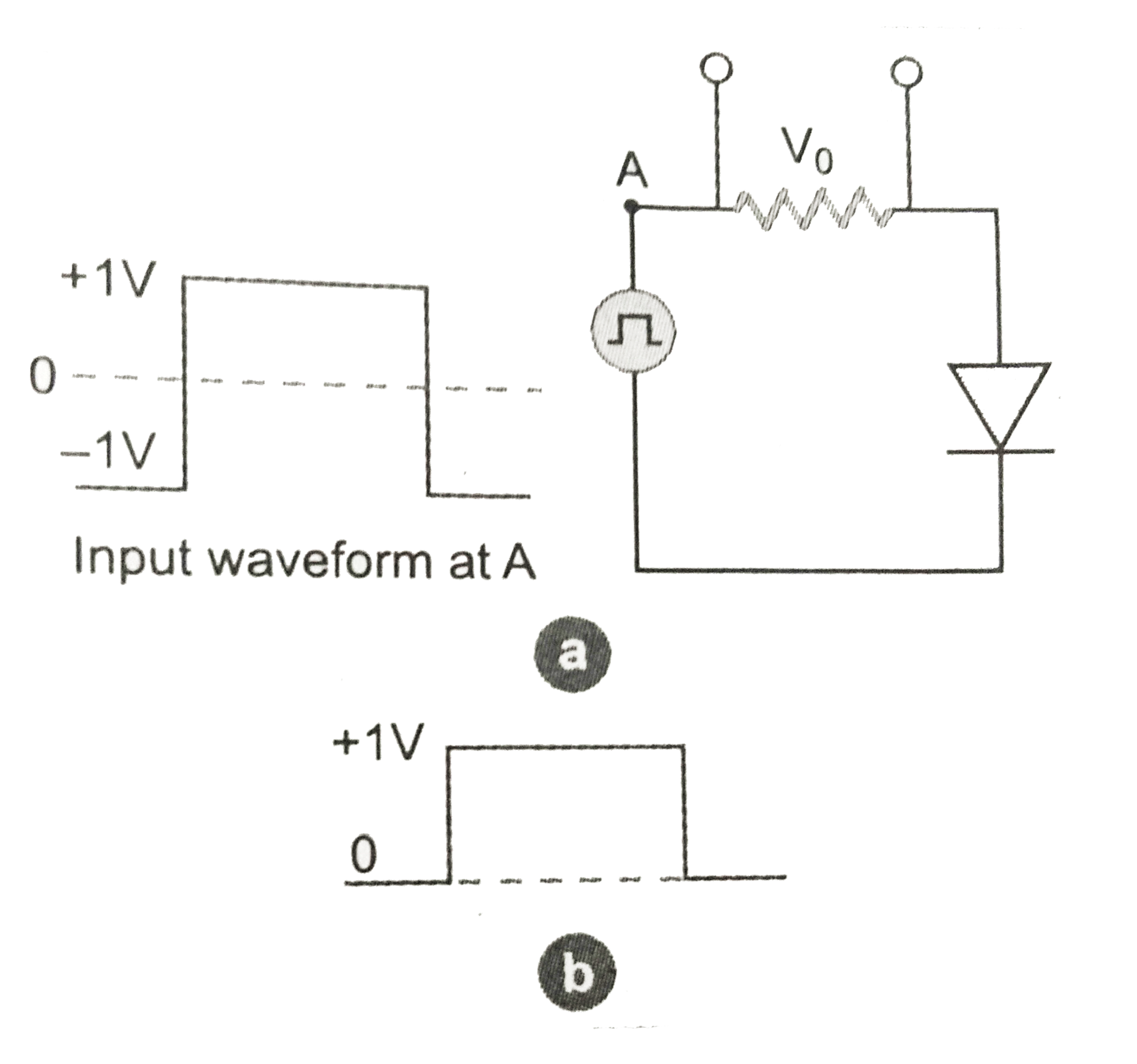
View SolutionThe figure shows the input weveforms A and B for 'AND' gate Draw the output waveform and write the truth table for this logic gate
 .
.
View Solution
