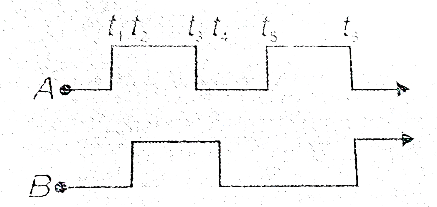
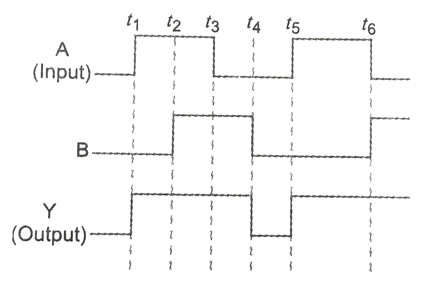
Show the output waveform of OR gate for the following input waveforms of A and B

(##AAK_P7_NEET_PHY_SP7_C29_E01_025_S01.png" width="80%">
Topper's Solved these Questions
- BOOK - AAKASH INSTITUTE ENGLISHCHAPTER - SEMICONDUCTOR ELECTRONICS (MATERIAL, DEVICES AND SIMPLE CIRUITS )EXERCISE - EXERCISE20videos
SEMICONDUCTOR ELECTRONICS (MATERIAL, DEVICES AND SIMPLE CIRUITS )
- BOOK - AAKASH INSTITUTE ENGLISHCHAPTER - SEMICONDUCTOR ELECTRONICS (MATERIAL, DEVICES AND SIMPLE CIRUITS )EXERCISE - Assignment section -A (Objective Type Question)43videos
SEMICONDUCTOR ELECTRONICS (MATERIAL, DEVICES AND SIMPLE CIRUITS )
- BOOK - AAKASH INSTITUTE ENGLISHCHAPTER - SEMICONDUCTOR ELECTRONICS (MATERIAL, DEVICES AND SIMPLE CIRUITS )EXERCISE - Assignment SECTION - D (Assertion & reason type Question)10videos
SEMICONDUCTOR ELECTRONICS (MATERIAL, DEVICES AND SIMPLE CIRUITS )
- BOOK - AAKASH INSTITUTE ENGLISHCHAPTER - RAY OPTICS AND OPTICAL INSTRUMENTSEXERCISE - ASSIGNMENT (SECTION - D)16videos
RAY OPTICS AND OPTICAL INSTRUMENTS
- BOOK - AAKASH INSTITUTE ENGLISHCHAPTER - SEMICONDUCTOR ELECTRONICS: MATERIALS, DEVICES AND SIMPLE CIRCUITSEXERCISE - Assignment (Section-D (Assertion and reason))5videos
SEMICONDUCTOR ELECTRONICS: MATERIALS, DEVICES AND SIMPLE CIRCUITS
Similar Questions
show the output waveform of AND gate for the following input waveforms of A and B.
 View Solution
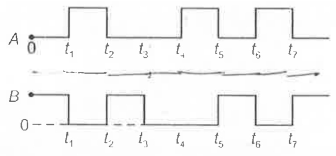
The output waveform of AND gate for the following input waveforms is
 View Solution
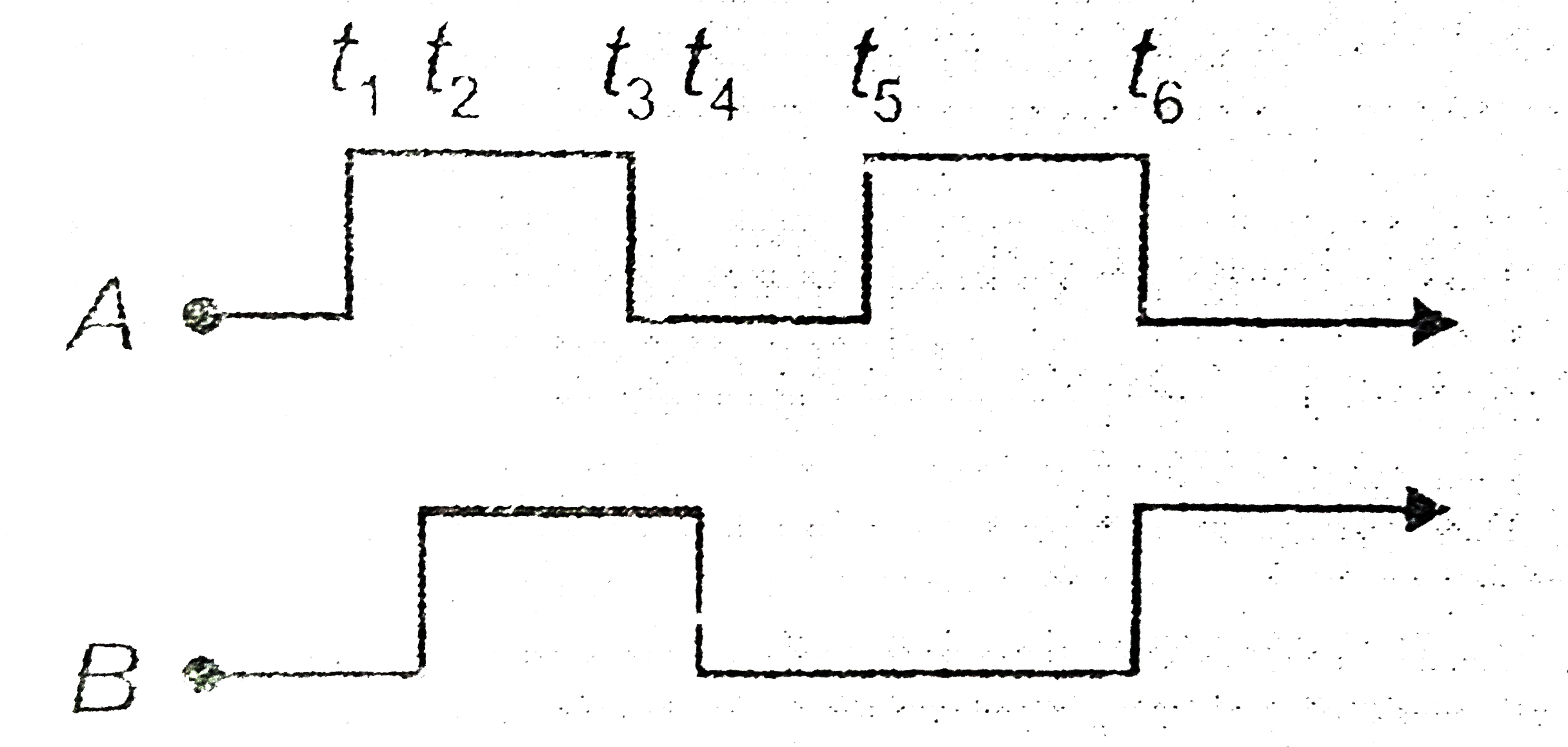
Sketch the output waveform obtained from AND gate for the following inputs A and B.
 View Solution
(a) Draw the circuit diagram of a full wave rectifier using p-n junction diole. Explain its working and show the output, input waveforms.
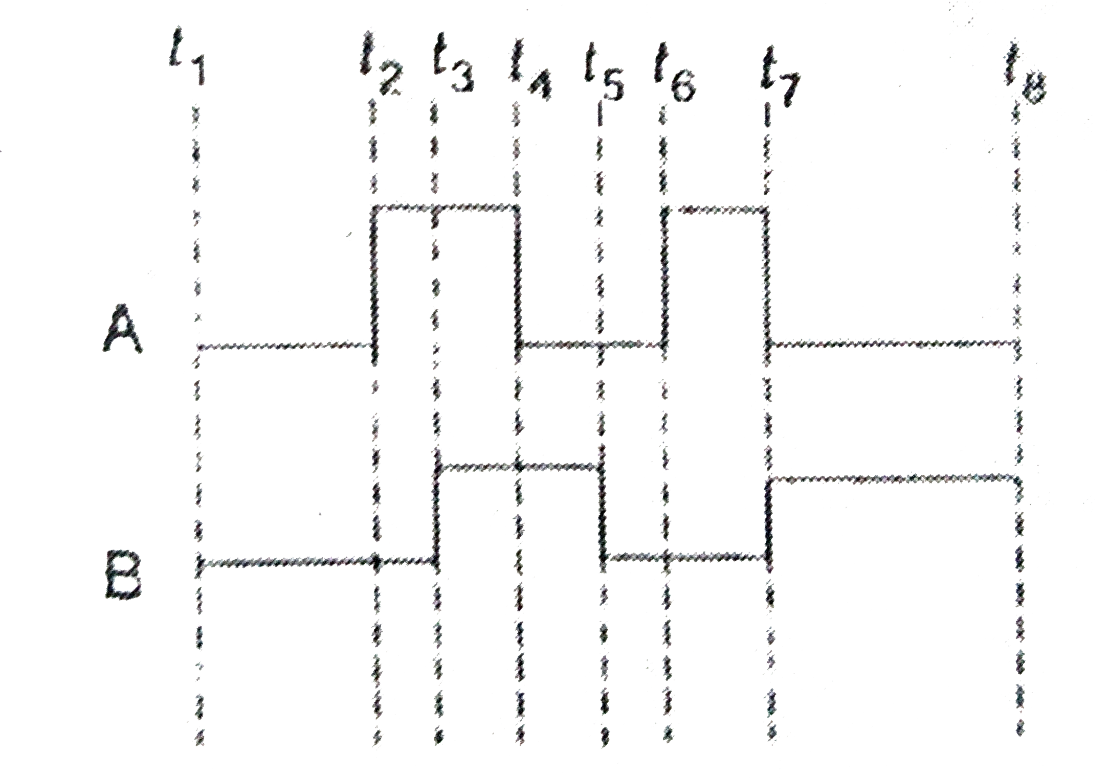
(b) Show the output waveforms (Y) for the following inputs A and B of (i) OR gate (ii) NAND gate :
 View Solution
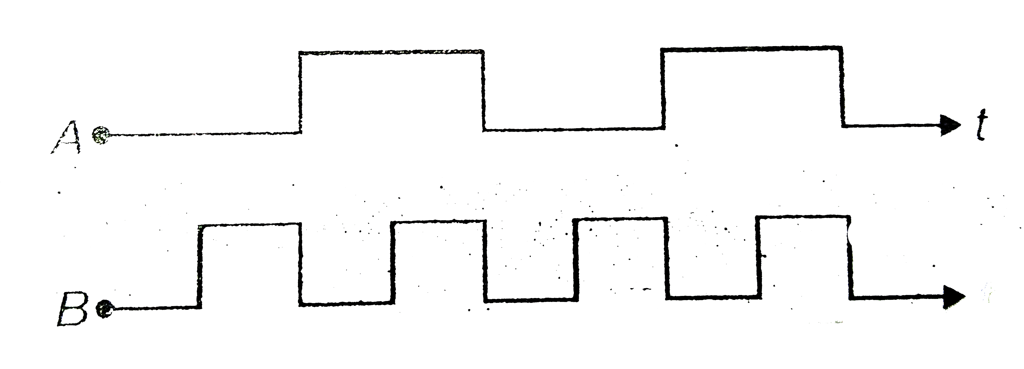
Sketch the output waveform Y from a NAND gate having following inputs A and B
 View Solution
Sketch the output wavefrom Y from a NAND gate having following inputs A and B
 View Solution
(i) Sketch the output waveform from an AND gate for the inputs A and B shown in the figure.
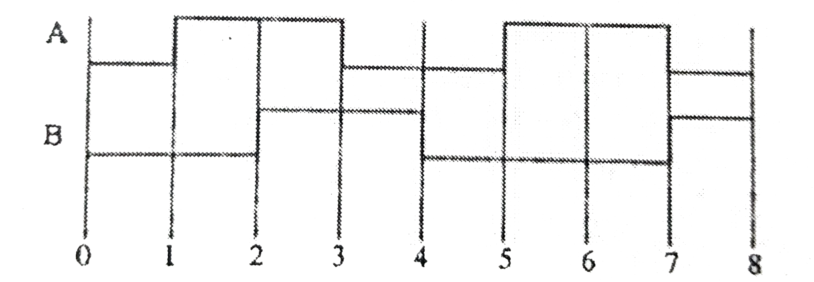
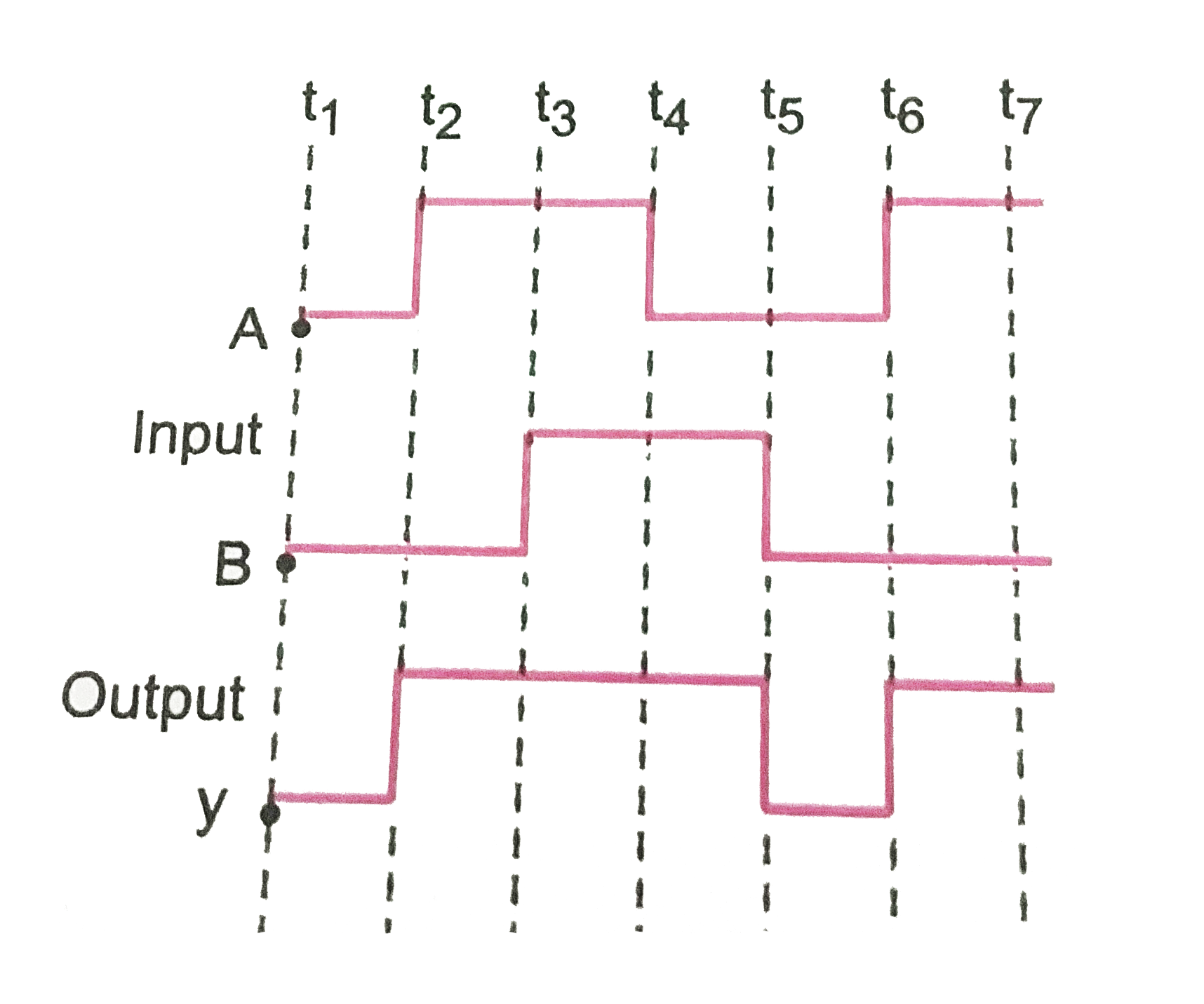
(ii) If the output of the above AND gate is fed to a NOT gate, name the gate of the combination so formed.View SolutionThe Fig shown input waveforms A and B to a logic gate. Draw the output waveform for an OR gate. Write the truth table for this logic gate and draw its logic symbol.
 View Solution
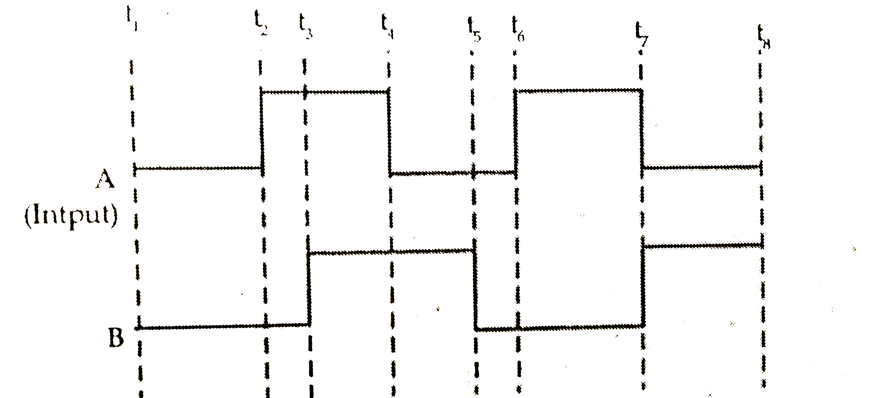
The figure shows the input weveforms A and B for 'AND' gate Draw the output waveform and write the truth table for this logic gate
 . View Solution
Justify the output wavefrom (y) of the OR gate for input and as gives in Fig.
 View Solution
