In the figure, the input waveform is converted into the output waveform by a device X. The devise X is a/an

amplifier
half wave rectifier
full wave rectifier
oscillator
The correct Answer is:C
Step by step video, text & image solution for In the figure, the input waveform is converted into the output waveform by a device X. The devise X is a/an by Physics experts to help you in doubts & scoring excellent marks in Class 12 exams.
Updated on:21/07/2023Topper's Solved these Questions
- ELECTRONIC DEVICESBook:MTG GUIDEChapter:ELECTRONIC DEVICESExercise:AIPMT/NEET (MCQs)
Explore 42 Videos
- ELECTRONIC DEVICESBook:MTG GUIDEChapter:ELECTRONIC DEVICESExercise:NEET CAFÉ (TOPICWISE PRACTICE QUESTIONS)
Explore 120 Videos
- ELECTROMAGNETIC WAVESBook:MTG GUIDEChapter:ELECTROMAGNETIC WAVESExercise:AIPMT/NEET(MCQs)
Explore 15 Videos
- ELECTROSTATICSBook:MTG GUIDEChapter:ELECTROSTATICSExercise:AIPMT/NEET (MCQ.s)
Explore 34 Videos
Similar Questions
Write the output waveform for the gates
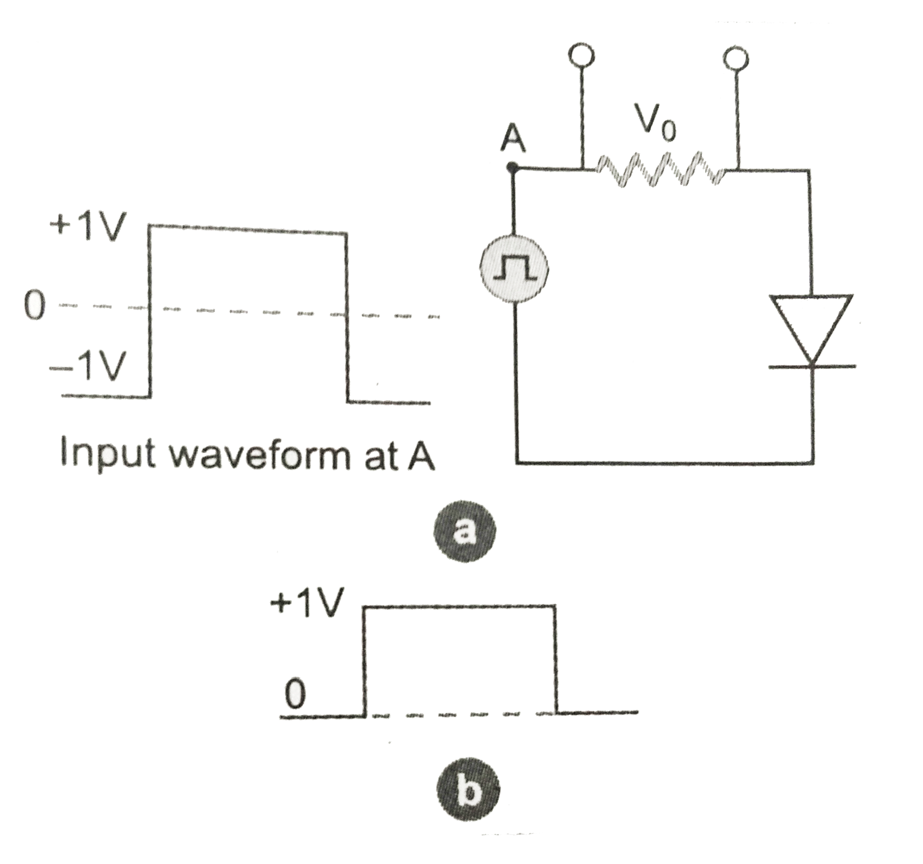
View SolutionDraw the output waveform across the resistor (Fig.)
View SolutionWrite the output waveform of the OR gate for the inputs
View SolutionIn the figure, the input is across the terminals
A and C and the output is across B and D. Then the output is
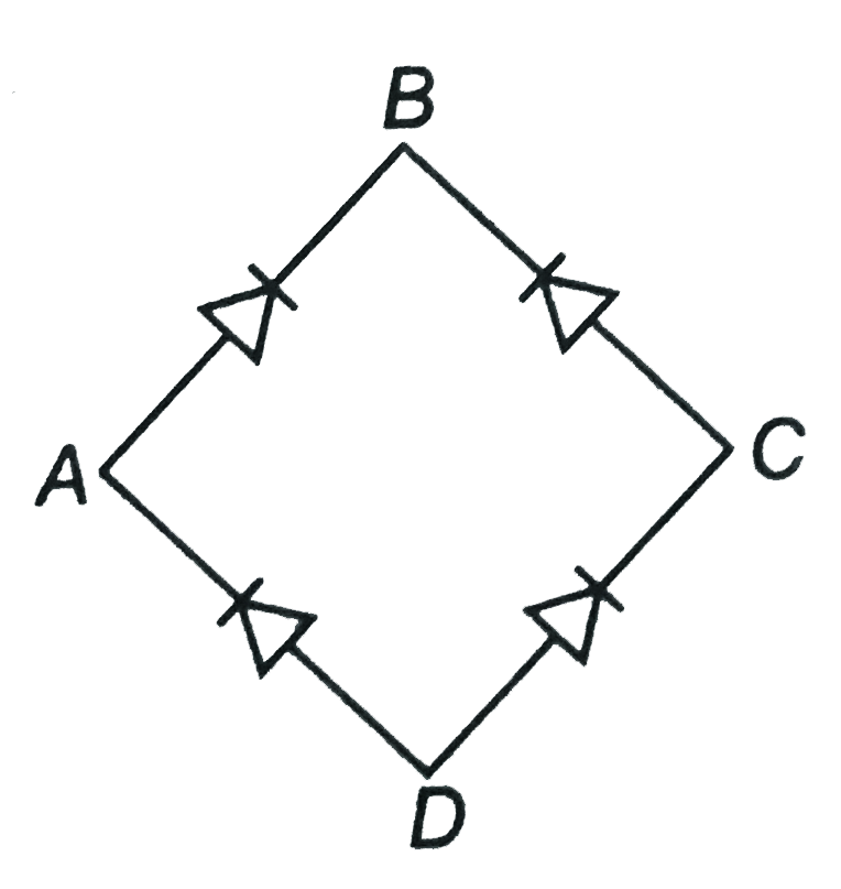
(a ) zero
( b) same as the input
( c) full - wave rectified
(d) half - wave rectified .
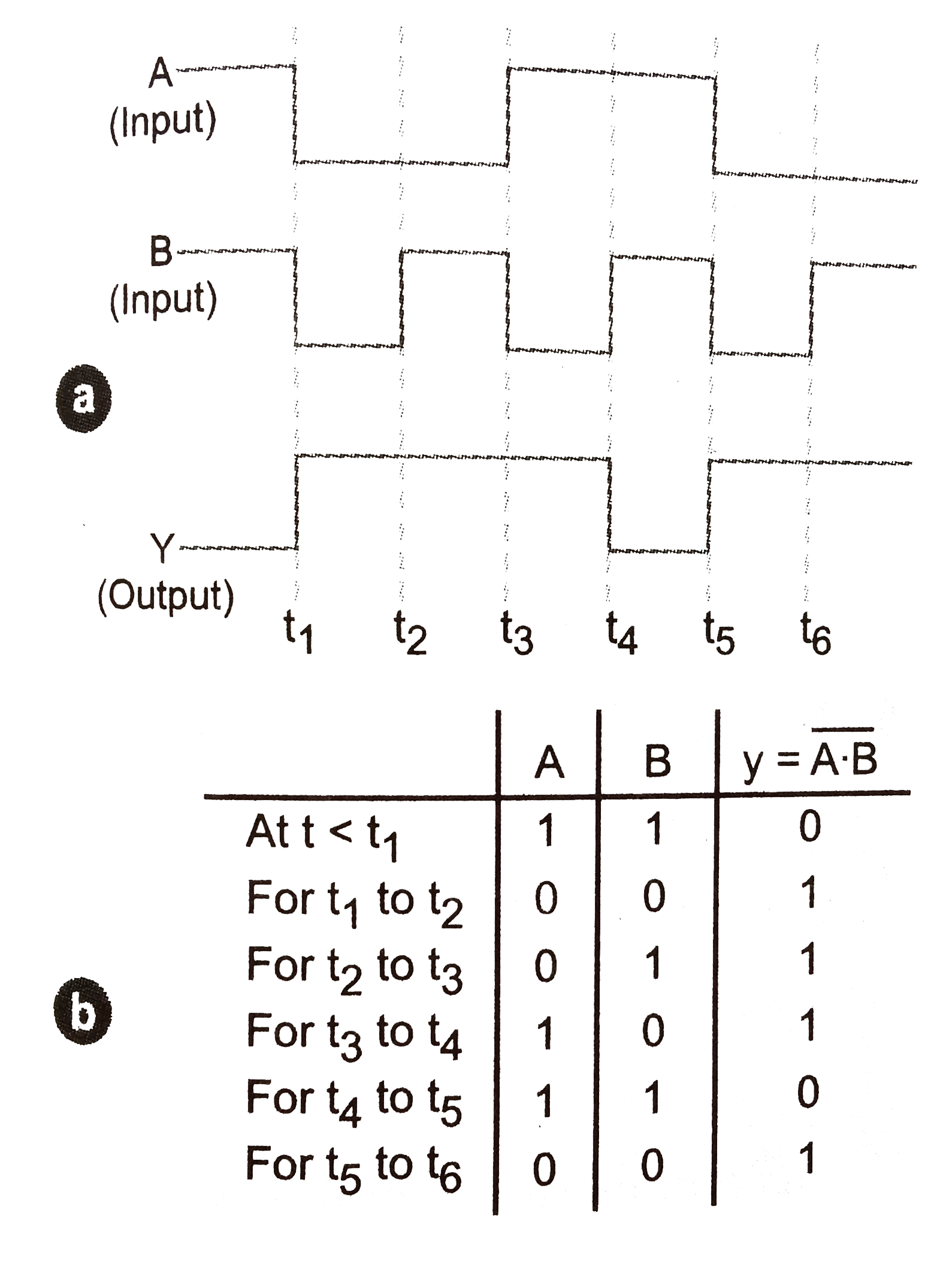
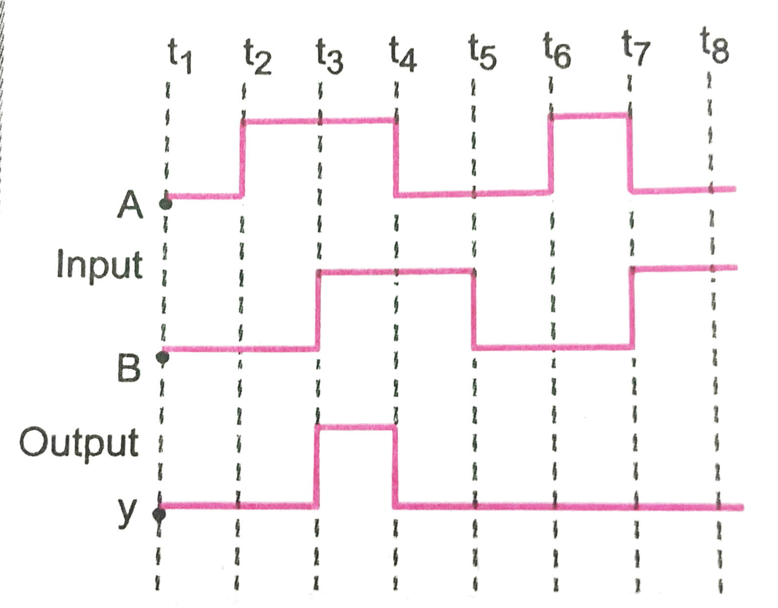
View SolutionThe following Fig. shows the input waveforms (A,B) and the output waveform (y) of a gate. Identify the gate and write its truth table.
View SolutionShow the output waveform of OR gate for the following input waveforms of A and B

View Solutionshow the output waveform of AND gate for the following input waveforms of A and B.

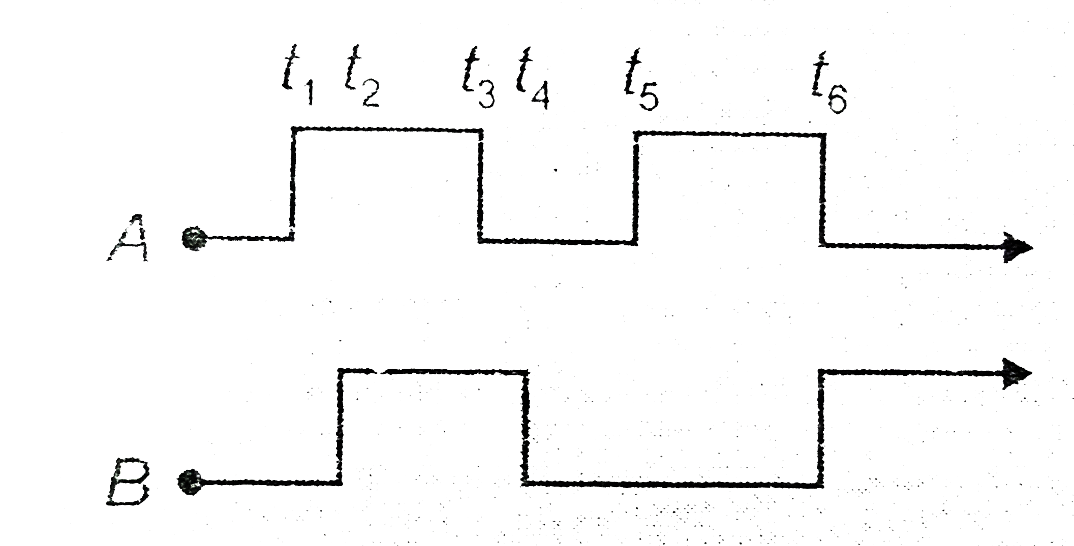
View SolutionShow the output waveform of OR gate for the following input waveforms of A and B
View SolutionDraw and explain the output waveform across the load resistor R, if the input waveform is as shown in the given.
View SolutionThe Fig.shows the input wavwforms A and B for 'AND' gate. Draw the output waveform and write the truth table for this logic gate.
View Solution

